
The "SSQ-2"
May 24, 2001
Revised to correct schematic errors on August, 2004
By Ralph M. Hartwell II
OVERVIEW:
Rife/Bare radiant tube systems are driven by a square wave modulated RF source. Generating accurate square waves is not as easily accomplished as is generating sine waves. With the advent of computer software which allows frequency accurate generation of sine waves along with the emergence of portable MP3 players and CD players, it is now possible to design a compact and portable Rife/Bare system which does not require an expensive frequency generator. Instead, the system may use a frequency sequence which has been previously created and saved on a music CD or as a series of MP3 files. These files may then be played back on a portable player or from a computer. The sine wave signal is then sent through a conversion process which converts the sine wave to a clean, symmetrical square wave. The square wave is then sent to the Rife/Bare system.
For more information on using MP3 files to control Rife/Bare systems, please, click here.
Due to the much higher bandwidth required to record square waves, it is preferable to record the frequencies as sine waves. By doing this, it is possible to record frequencies between 1 Hz and 20 kHz on a standard music CD. The quality of the playback will depend on the characteristics of the particular CD player or computer sound card used. The sine wave signal played from the CD or MP3 file must then be sent through a processing circuit which will convert the sine wave to a clean, symmetrical square wave for use with the Rife/Bare system.
THE PROBLEM:
I wanted to design a simple, effective circuit which would convert the sine waves available from a CD player or an MP3 playback system into accurate square waves suitable for driving a Rife/Bare modulation system.
Circuits which convert sine waves to square waves have a particularly difficult task to perform. If it is required that the square wave needs to be symmetrical and have low phase jitter, then the circuit must compensate for such things as noise on the incoming signal and waveform distortion. The standard approach is to use a Schmidt Trigger circuit in an attempt to eliminate the noise and reduce phase jitter. While this approach works fairly well in most cases, it can also require substantial signal conditioning prior to the Schmidt Trigger circuit itself.
My first attempt at waveform conversion "Signal Slicer" was an attempt to be an "all things to all signals" design. It attempted to handle large signal amplitude swings, as well as distorted sine wave input signals. While it did indeed perform well, it suffered from unwanted internal noise which tended to cause phase jitter, particularly when operating at low frequencies. The circuit also tended to have less than perfect output waveshape symmetry at frequencies above 12,000 Hz. In the absence of an input signal, the circuit sometimes oscillated at high frequencies. This would would cause an unwanted output signal to be generated. In the presence of a large amount of high frequency noise, the circuit occasionally exhibited more phase jitter than was desired.
Tests of various CD players showed that many of them have a rather large supersonic noise component which could interfere with the correct operation of a sine to square wave converter.
A NEW DESIGN:
The circuit described in this article is an attempt to remedy some of these problems and produce a design aimed specifically for use with portable CD/MP3 players and computer sound cards.
The first attempt at designing a wave shape converter simply used one stage of a 74HCT240 digital buffer IC to turn the sine wave into a square wave.
Most people are not aware that most digital circuits are, in fact, actually very high gain analog amplifiers. By properly biasing (from an analog viewpoint) the input gate of the IC, it is possible to obtain an analog amplifier with extremely high gain. When a varying signal is applied to the input of this rebiased amplifier, the output will change from full on to full off whenever the input signal crosses the bias voltage threshold. By doing this, I was able to feed a sine wave into the IC, and recover a square wave from the output. While this approach worked fairly well, it did have the problem of being somewhat level-dependent with regard to the input sine wave signal, and it also appeared to have excessive phase jitter.
Further tests showed that most of this problem was related to the fact that there was a lot of high frequency noise in the region of about 50 kHz coming from the CD player. This, combined with the slow rise time of the sine wave, especially at low audio frequencies, cause the input signal to fluctuate in and out of the critical bias voltage region as the sine wave was ramping up or down during the audio cycle. It proved impossible to filter the high frequency noise out of the signal and still get a symmetrical square wave out of the IC at all frequencies and input voltage levels.
The solution tuned out to be a form of active filtering, where the signal was simply amplified to a much greater degree by using a separate amplifier, then shaping the amplifier's frequency response to obtain the correct square wave output. The additional amplification also corrected the slow rise time of the input square wave as sent to the digital IC.
CIRCUIT DESIGN:
The circuit is a two-chip design, using readily available components. Suppliers such as Radio Shack, Digi-Key, Mouser Electronics and others will have these parts available. The unit may be battery powered or operated from the AC power line using a standard "wall-wart" power module. The circuit board, if carefully built, will fit inside most any CB radio.
The unit will operate between 2 Hz and 23 kHz. This frequency range encompasses the entire frequency bandwidth that a music CD or MP3 file can handle. Although the preferred input signal level to the circuit is between 0.2 to 0.4 Volts peak-to-peak, it will operate with signal levels a low as 0.05 Vpp and as high as 1.0 Vpp. Operation beyond those levels will not damage the circuit, but will result in unstable output, missing pulses, non-symmetrical waveform output and frequency doubling.
For the following discussion, please refer to the circuit diagram shown here.
Click here for a PDF copy of the schematic diagram.
CIRCUIT OPERATION:
The power supply is straightforward, and uses a zener diode regulator instead of a more conventional three-terminal voltage regulator IC. The use of the zener diode results in almost total immunity to outside RF interference to the voltage regulator. It also prevents catastrophic failure of the IC's in the event of a construction error or operating problem due to the inherent current limiting provided by the four series voltage dropping resistors in the regulator circuit.
DC power in the range of 9 to 20 volts is applied to the power terminals. This voltage is filtered by the 220 uf 35 v electrolytic capacitor. The filtered DC voltage passes through 4 - 68 ohm 1/2 watt dropping resistors. These resistors are connected to the zener diode which regulates the DC voltage to +5 volts. The 6.8 uf capacitor acts as a noise filter and bypass capacitor. The regulated +5 volts is then connected to the two integrated circuits.
The first stage of the wave shaper uses a conventional low frequency operational amplifier. This amplifier is configured so as to have a very large amount of gain. This high gain causes the incoming sine wave to be amplified well past the point of clipping. The result is that there is a semi-square wave appearing at the output (pin 1) of the op-amp.
The incoming sine wave audio input signal is fed into the non-inverting input of the LM324 Op-Amp through a high pass filter composed of a 270 ohm resistor, a 220 uf capacitor and a 680 ohm resistor. This filter eliminates any very low frequency signals below about 1/2 Hz. The gain of this circuit is controlled by feedback resistors of 120 k and 330 ohms. A 100 pf capacitor is used to suppress high frequency noise generated in the '324 at high gain values. The circuit voltage gain is approximately 350, and may be adjusted for different signal input voltage values by changing the value of the 330 ohm resistor.
The amplified and peak-clipped sine wave signal appears at output pin 1 of the '324 op-amp, and is then coupled into the inputs of four sections of the 74HCT240 buffer amplifier. The 100 k series coupling resistor limits the drive current fed to the '240, while the 470 pf coupling capacitor adds some additional high frequency coupling between the amplifier and the digital IC. The extra "punch" provided by this capacitor helps to ensure that the switching transitions in the '240 occur at a high speed. This helps to reduce phase jitter in the square wave output.
Four of the eight available sections of the 74HCT240 are paralleled to obtain a high drive current at the main output of the circuit. The output appears as a 0 to +5 volt signal having a 50 ohm source impedance. This output may be used to drive a length of 50 ohm coaxial cable or may be sent to a higher resistance load, such as a potentiometer or other amplifier. If a coax cable is used, its far end should be terminated in 50 ohm load to prevent signal reflections from the end of the line which would cause distortion of the rising and falling edges of the square wave signals.
The main output signal is also fed into the fifth section of the '240. The output from this buffer appears as a lower power, 0 to +5 volt signal having a 50 ohm source impedance. This signal may be sent to a signal monitor, audio amplifier, frequency counter, oscilloscope, etc., for signal quality monitoring.
The main output signal is also fed into the sixth section of the '240. The output from this buffer appears as a lower power, 0 to +5 volt signal. It is then sent to a series dropping resistor, (R) and then to the hot side of the variable potentiometer (VR). By selecting the correct value of (R), the output signal from the potentiometer (VR) may be adjusted between zero and a maximum of either 260, 450, or 1020 millivolts. These voltage levels are suitable for driving a modified CB radio microphone circuit for Rife/Bare operation. Refer to the small notes block on the diagram for the appropriate value for (R).
Note that the pictures of the assembled unit do not show resistors (R) or (VR) or the microphone drive connections. Since I am not using that portion of the circuit, I did not build it into the unit which is shown here.
CONSTRUCTION:
The circuit is constructed on readily available perf-board. Because we are dealing with high frequencies here, it is suggested that good construction practices be used. This means keeping all leads as short as possible, bypassing power leads if and when necessary, and using shielding as needed.
It is necessary to connect all of the inputs of the unused sections of the 74HCT240 to the negative terminal of the power supply to prevent spurious oscillations from occurring.
Shown below is the front and back view of this circuit as built for the prototype. It worked correctly the first time it was tested. No attempt was made to build the circuit board as small as possible. From the pictures, it is apparent that the size could be reduced considerably if needed.
Note that there is a slight labeling error on this board - can you spot it? <G>


Here's the board as it is installed in a plastic project box. Note the very small amount of wiring required to connect the board to the connectors and power supply wires.

The finished wave shaper ready for use!
Have a look at the results!
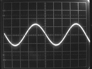
10 kHz sine wave input signal, amplitude is 0.25 V peak-to-peak.
Notice the high frequency noise present on the sine wave. This comes from the internal circuits of the CD player, and is almost never noticed when listening to music with the CD player, as this noise is well above the range of normal hearing. Unless it is removed, this noise will interfere with the operation of a circuit designed to convert sine waves to square waves.

20 kHz square wave output signal, amplitude is 5 V peak to peak.
Notice the very fast rise and fall times of the waveform.

30 Hz square wave output signal, amplitude is 5 V peak to peak. Notice the good waveform symmetry even at this low frequency.

15 Hz square wave output signal, amplitude is 5 V peak to peak. The signal is just as good as it was at 30 Hz. The output continues to remain very clean and symmetrical right down to 2 Hz, but I was not able to take any scope photos because my digital camera will not handle shutter speeds slow enough to capture waveforms at that frequency. Trust me though; it works!
[ Home ]