A KW Switch Mode Regulated High Voltage Power Supply
By W5JGV
Last Updated September June 8, 2005
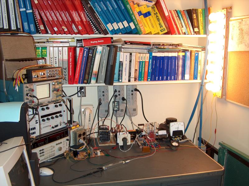
Bench Testing of the Switching Power Supply
SAFETY WARNING!!
This unit handles voltages and currents that can be INSTANTLY LETHAL upon contact. Both the input and output ends of the unit are dangerous, as they both contain high voltages and are capable of high currents.
IF YOU DO NOT HAVE EXPERIENCE IN WORKING WITH HIGH VOLTAGES, THEN DO NOT ATTEMPT TO CONSTRUCT THIS POWER SUPPLY WITHOUT THE GUIDANCE OF A PROPERLY QUALIFIED INSTRUCTOR.
DEATH IS PERMANENT
PLEASE BE CAREFUL!!
The data sheets listed below are all in Adobe PDF format.
I suggest that you download these files for reference while reading the circuit description.
Click HERE for the schematic diagram of the 120 Volt unit.
Click HERE for the parts list for the 120 Volt unit.
Click HERE for the schematic diagram of the 240 Volt unit.
Click HERE for the parts list for the 240 Volt unit.
Click HERE for the data sheet on the TL494 switching controller IC.
Click HERE for the data sheet on the TL594 Switching controller IC.
Note: the ON Semiconductor version of the TL594 is a higher powered version of the more common TL494 and is a better choice for this circuit because it will provides higher IGBT drive capability. It also has a low voltage lockout circuit, which is not required for this power supply. The output transistors in the TL594 are rated at 500 ma, whereas the TL494 is rated at only 200 ma. However, the TL594 that is manufactured by Texas Instruments has the same current ratings as the standard TL494, and therefore has no particular advantage over the TL494. If you do use a TL594 in place of the TL494, it may be used with no circuit changes required.
Click HERE for the data sheet for the HGTG27N120BN power transistor.
Click HERE for the data sheet on the UF4007 diode.
Click HERE for the data sheet on the Ferroxcube "U" transformer core.
Click HERE for the data sheet on the Ferroxcube "I" transformer core.
The following files are useful as reference material if you want to design your own switching power supply:
Click HERE for "Topologies for Switched Mode Power Supplies"
Click HERE for "ON Semiconductor SMPS Power Supply Design Manual"
Click HERE for the "Fuji IGBT Application Manual REH984"
Click HERE for "Design of Magnetic Components"
Click HERE for "Inverter Transformer Design and Core Selection"
Click HERE for "Reactive Elements in Switched Power Conversion"
Click HERE for "Wakefield Heatsink Thermal Tutorial"
The following files were added on June 8, 2005
Click HERE for "Choose Wisely" IGBT or MOSFET selector"
Click HERE for "IGBT Basics" by Motorola
Click HERE for "IGBT Basics by Fairchild
Click HERE for "Introduction to IGBT Operation"
Click HERE for "IGBT Gate Drive for Maximum Efficiency"
Click HERE for "Stranded Wire as a Substitute for Litz Wire in Transformers"
NOTICE: Copyright on the above listed Data Sheets and Application Manuals remain with the original copyright holder. No claim to any portion of said copyright is made or inferred by the operator of this Web Site.
The following files are in MPG format. They show the power supply 3 second startup cycle.
Click HERE for a wide view video of the startup showing the lamp load
Click HERE for a video of the voltage and current meters during startup
Click HERE for a video of the PWM waveform during startup
OVERVIEW
This intent of this article is to provide useful information so that a copy of this power supply, or one similar is design may be built by an experienced experimenter or Amateur Radio Operator using the components and techniques specified here. The concepts and techniques described here may also be used to assist the experimenter in designing his or her own switching power supply. With few exceptions, most of the components used in this circuit may be substituted with other components, depending on the depth of the experimenters junk box.
The design of switching supplies is a bit more involved than traditional "big iron" transformer power supplies. When taken step-by-step, however, it is quite possible for an amateur to design and build a working high power switching power supply. This article describes a high power, high voltage switch mode power supply designed to operate a KW level RF power amplifier.
This power supply was designed to replace the original power supply in a Heath Warrior power amplifier which uses 4 - 811A tubes. With some minor modifications, this amplifier may be pushed to the maximum tube rating in SSB service. This requires a plate voltage of 1500 volts and a per tube plate current of 175 milliamperes.
SPECIFICATIONS:
SUMMARY OF OPERATION
The AC mains voltage is rectified and filtered into DC. The DC is then chopped up by a pair of power transistors into a string of alternating positive and negative 130 volt pulses at a frequency of 27 kHz. These pulses are sent to to a step-up transformer and transformed into a 1,600 volt AC square wave. The 1,600 volts is rectified and filtered into DC to power the load. A sample of the 1,600 volt output is used to control a pulse width modulator (PWM) which adjusts the width of the pulses that are sent to the step-up transformer. By adjusting the width of these pulses, the PWM controls the amount of power available to the load. The PWM adjusts the pulse width so that the filtered DC output voltage remains constant as the load or mains voltage changes. Suitable protection is included so that the supply will not suffer a catastrophic failure in the event of an overload or accidental short circuit across the output terminals.
DETAILED DESCRIPTION:
Please refer to the schematic diagram of the power supply for the following discussion. You may use either the 120 volt or the 240 volt version, as the only difference is in the AC mains area of the schematic diagrams.
AC INPUT AND RECTIFIERS:
Primary mains power enters the power supply through a line filter FL1, which is designed to prevent RF noise which may be generated by the power supply from getting into the power lines and causing interference. I used a filter salvaged from a large computer power supply. The mains voltage is then rectified and used to charge a pair of primary DC power filter capacitor banks.
Each of the filter banks, C3 and C4 are made from 6 - 680 uF electrolytic capacitors connected in parallel for a total capacity of 4080 uF at 200 VDC. Both filter banks are identical. Because of the high value of ripple current passing though these capacitors, these filter banks use capacitors which are designed for computer switching power supplies. I used capacitors salvaged from some old 250 watt computer power supplies. One filter bank will be charged to plus 130 volts DC and the other filter bank will be charged to minus 130 volts DC by the rectifier.
Note that the 120 volt version uses dual half-wave rectifiers D1 and D2 which charge each capacitor bank on opposite polarities of the AC mains wave. The 240 volt version uses diodes D1, D2, D55 and D56 which are connected as a full-wave bridge rectifier. In the 240 volt version, the mains voltage charges both capacitor banks at the same time, but with opposite polarities. This means that the 240 volt version will have double the mains ripple frequency, and a lower ripple amplitude than will the 120 volt version. Fuse F1 in the 120 volt unit and F1 and F2 in the 240 volt unit protect the unit from mains overloads.
A pair of 4 watt, 130 volt light bulbs Y1 and Y2 are connected across each capacitor bank, These lamps serve to provide a visual indication of the presence of rectified mains voltage and also act as bleeder resistors for the primary filter capacitors and to discharge the primary filters when the mains power is removed.
Inrush mains current surge protection is supplied by resistor R6 in the 120 volt unit, and by resistors R6 and R34 in the 240 volt unit. The surge resistors are bypassed by the normally open contacts of relay K1 after the pre-charge time delay supplied by time delay relay K2. K2 starts its timing cycle when AC mains power is applied by closing switch S1 to begin charging the main DC filter capacitor banks.
HALF-BRIDGE SWITCHER:
The power supply uses a half-bridge power switching circuit. In this design, one side of the primary winding of switching transformer T2 is connected to the primary DC power common return point, (the junction of C3 and C4) and the other end of the primary winding is connected to the emitter-collector junction of the two switching transistors. The transistors are connected and driven such that one transistor will switch +130 volts to the primary winding of the transformer, and the other transistor will switch -130 volts to the primary winding of the transformer.
NOTE: In the 120 volt version, this common point is connected directly to one side of the mains supply. In the 240 volt version, the common point will be connected to the mains common return line, which normally will be at earth potential, but don't count on that as always being true. Safety first - check everything and stay alive!
One of the two switching transistors mounted on its heat sink.
The transistor shown here is Q2. Each transistor is mounted on a separate heat sink. No insulating spacer is used between the transistors and the heat sinks, as it is necessary to ensure that the transistors remain as cool as possible to prevent the increased losses which occur at elevated temperatures. A terminal strip is placed by each of the switching transistors. The terminal strip is used to hold the spike suppressor diodes D3 and D4. The heavy red wire connects the collector of Q2 to the emitter of Q1.
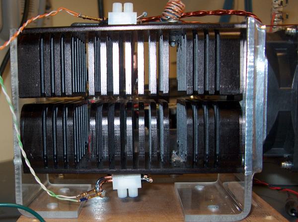
This is a side view of the heat sinks as they are assembled in the power supply.
Since there is 130 volts difference in potential between the two heat sinks, they are mounted on a pair of insulating angle brackets which are made from 1/4" thick clear plastic sheet. The heat sinks themselves are salvaged from some used Pentium II processors. The heat sinks are separated slightly so that there is no electrical contact between them.
A small cooling fan, which was salvaged from an old computer supply, is attached to the plastic bracket which holds one end of the heat sink assembly. The plastic bracket has an opening cut into it so that the cooling air from the fan will pass lengthways through the heat sink. Heated air flows outwards horizontally from the heat sinks.
Note the aluminum foil tape which is used to hold the fan against the plastic bracket. If you mount the fan in this manner, make sure that the aluminum foil does not short circuit the two heat sinks!! Since these heat sinks are at 130 volts above earth potential, the foil should not contact either heat sink. For safety, be sure to protect the heat sinks from accidental contact by the operator or bystanders.
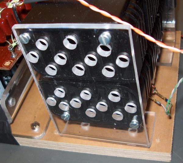
This bracket is attached to the end of the heat sink assembly opposite the cooling fan.
Notice the holes that have been drilled through the plastic bracket. These holes are there to allow some of the heated air to escape from the end of the heat sink, otherwise there would be a dead air pocket at this end of the heat sink which would have reduced the cooling efficiency of the heat sinks.
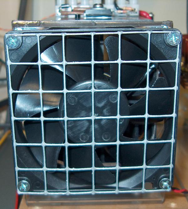
Home brew fan guard.
The edges of the blades on the cooling fan are sharp - trust me on that! I fashioned a fan guard from a small section of "hardware cloth" which has 1/2" spacing between the wires. By chance, it turns out to be a perfect fit between the mounting screws, which, when screwed into the mounting holes, holds the hardware cloth firmly in place.
POWER SWITCHING TRANSISTORS:
Now that we have the primary + and - 130 volt DC power available, we must transform it to 1,500 volts. To do so, we use a pair of high voltage, high current IGBT's (Insulated Gate Bipolar Transistors) to create a 130 volt AC waveform by alternately switching the plus and minus 130 volts DC from the primary filter capacitors into a ferrite core step-up transformer. This transformer steps up the 130 volt AC signal to approximately 1,600 volts AC on the secondary winding of the transformer.
The transistors Q1 and Q2 that are used for this task are Fairchild type HGTG27N120BN IGBT devices, which are rated at 1,200 volts and 72 amperes. After reading the fine print in the data sheets, we see that these are the maximum ratings at for operation at DC, but when we operate them at higher frequencies, the allowable current drops considerably. In the unit described here, the transistors are operating at 27 KHz, which reduces the allowable current to about 15 amperes. That is more than sufficient for our needs. The 1,200 volt rating applies regardless of the operating frequency. The 1,200 volt rating also gives the supply excellent protection against transistor failure due to voltage spikes. Other IGBT or MOSFET transistors could be substituted for the transistors used here, as long as they have a voltage rating of at least 600 volts and a current rating of 12 amperes or more at an operating frequency of 27 KHz.
The switching transistors are protected against reverse voltage spikes by the use of fast switching UF4007 diodes D3 and D4 which are placed across the emitter and collector of transistors Q1 and Q2.
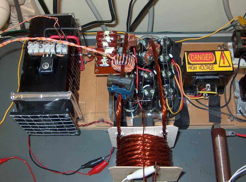
The "Heart of The Switcher"
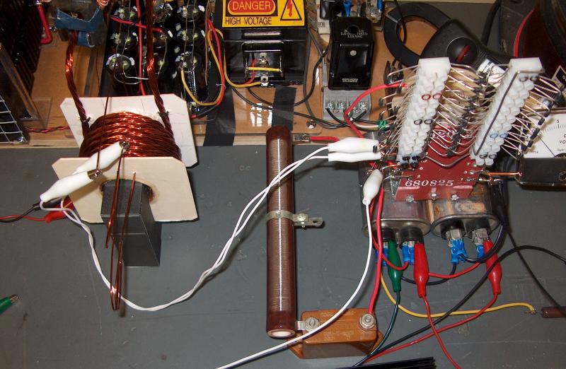
This shows one of the two IGBT power switching transistors which are mounted on their individual heat sinks, (The other switching transistor is mounted underneath the heat sink assembly,) the filter capacitor banks, the DC blocking capacitor, the switching transformer, the mains rectifier on its heat sink, and the overcurrent sample transformer. The small square black ferrite core transformer seen in front of the overcurrent sample transformer is used to take a sample of the transformer current and send it to an oscilloscope so I can monitor it.
SWITCHING STEP-UP TRANSFORMER:
Transformer T2 is used to step up the 130 volt AC signal generated by transistors Q1 and Q2 to about 1,600 volts AC. Because of the 27 KHz switching frequency used in this system, a laminated iron core would exhibit excessive hysteresis losses. A ferrite core is used instead. Because a power level in excess of 1KW was required, a fairly large core was used. It would have been possible to use a smaller size core, since the one used here is capable of power levels in excess of 4KW, however using this large core allows the use of a relatively small number of turns of wire on the transformer, thereby reducing copper losses. In addition, the larger core has a greater window area, and allows much more leeway in placing the windings with plenty of space for cooling and insulation.
The operating frequency of 27 KHz was chosen for purely practical reasons. The higher the operating frequency, the smaller and lighter transformers are for a given power level. However, semiconductor losses tend to increase as the operating frequency is raised, and obtaining usable power transistors becomes more difficult and expensive. The power transistors used in this design were available at reasonable cost on the surplus market, and, if purchased new, cost less than USD $13.00 each. Since my first experiments were done using ferrite cores from LOPT's which operate at 15.75 KHz ,and with transformers salvaged from computer power supplies which operate between 40 and 100 KHz, it seemed that a frequency somewhere between 20 to 30 KHz would probably be suitable for use in this project.
The transformer core is assembled from two stock items from Ferroxcube. The part first is a "U" section, P/N U100/57/25-3C90, with a cross-sectional area of 6.45 cm^2. The second part of the core is an "I"-bar section, P/N I100/57/25-3C90, with the same cross sectional area. If additional core "window" area in needed to make room for more winding space, a second "U" section core may be substituted for the "I"-bar section with no loss in performance.
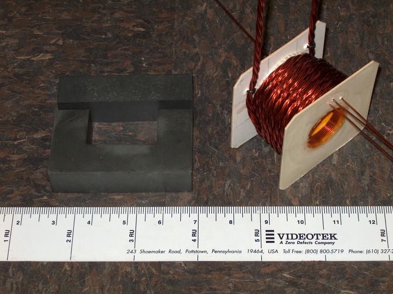
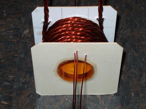
The picture shows the size of the core sections and the completed transformer coil.
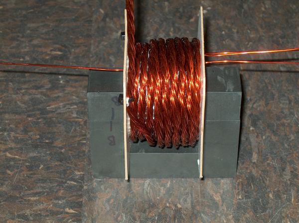
The core sections as they are fitted to the coil.
SWITCHING TRANSFORMER CONSTRUCTION DETAILS:
The windings were wound on a coil form which was then slipped over the "I"-bar and then the "U" section was simply placed against the sides of the "I"-bar to complete the magnetic circuit. The core sections are held together with several wraps of glass reinforced tape.
The coil form for the transformer was constructed by obtaining a length of thin walled plastic tube which would just slide over the "I"-bar core section. I used a yellow plastic pill bottle with the ends trimmed off. The tube was cut to length so that it just fit between the ends of the "U" core section. Two square pieces of artists art matte board were then cut to fit inside the window area available when the core sections were assembled. Using a sharp knife, a snug-fitting round hole was then cut in the center of each piece of matte board. The matte board end plates were then fitted to the ends of the tube by attaching them in place with cyanoacrylate adhesive
Next, the end plates were given three coats of liquid plastic cement to prevent then from absorbing moisture from the air. I used clear PVC pipe cement. I allowed each coat to dry for several hours before applying the next coat of cement.
After allowing the coil form to dry, the secondary winding was wound on the form. It consists of 205 turns of # 18 AWG wire. The wire is larger than actually required (21 gauge would be adequate) even after factoring in skin effect and current crowding at 27 KHz, but I had a lot of the # 18 gauge wire available, and since there was plenty of room on the coil form for it, it was used.
The secondary winding has an inductance of about 436 mHy with the ferrite core sections in place, and has a self-resonant frequency of about 35 kHz.
The finished Switching Transformer Windings.
You can see the primary winding on the outside of the coil, and visible through the yellow plastic pill bottle tube in the center of the coil form is the first layer of the high voltage secondary. Note that there are extra secondary wires shown here. Since this was the first unit built, I added an auxiliary secondary winding to allow me to be able to adjust the output voltage for testing.
The primary winding has an inductance of about 1.6 mHy with the ferrite core sections in place.
Another view of the completed coil.
It is necessary to minimize the winding self-capacity to keep the winding self-resonant frequency as high as possible. The self-resonant frequency must be higher than the switching frequency, or the transformer will not perform properly. To do this I applied two layers of fiberglass tape over each winding layer as I finished the layer.
NOTE: To measure the resonant frequency of the transformer, insert the core sections into the coil and fasten them together with tape. Make sure the primary winding is open circuited. Using an audio oscillator that will go up to about 70 KHz, feed a sine wave through a 22,000 Ohm resistor to the secondary winding. Monitor the signal level across the secondary winding with an oscilloscope and a 10X probe. Adjust the frequency of the audio oscillator until you find the lowest frequency at which the sample signal is greatest. The frequency at which this resonant rise occurs is the resonant frequency of the transformer. It must be above 27 KHz for proper operation of the power supply.
I then continued winding the next layer of the secondary by carefully folding the wire back across the previously finished winding layer so that the next layer started from the same side of the form where the previous winding began. This required extra insulation between the folded over wire and the windings to prevent insulation failure. I did this by applying an additional strip of insulating tape crosswise to the just-completed winding layer. This was placed directly under the folded across wire. Two thickness of insulating tape were then placed on top of the folded across wire and the next layer was carefully begun.
Note that it is vitally important to prevent a winding turn at the outer ends of the form from being "pulled under" and dropping down into the completed winding below the winding layer you are working on. If this happens, it is a sure invitation to an arc-over between layers and instant failure.
After completing the desired number of turns, the finished secondary winding was wrapped with several layers of insulating tape.
Because this text description of the winding process may not be easily understandable, I have illustrated the process with the following pictures and text. The illustrative winding shown in the pictures is not the actual transformer winding, but is used specifically to show the method of winding.
This illustrates the method of winding the secondary for minimum inter-layer capacity.
First, wind a layer on the coil form in the usual manner, with the layer close wound. In this example, the winding starts at the left side of the form and finishes at the right of the form. After finishing the winding layer, cover the winding with insulating tape. Note that for this example, I have used aluminized Duct Tape and plastic electrical tape, neither of which is actually suitable for the actual transformer. Use a Fiberglass tape instead. It will withstand heat and mechanical stress much better than plastic tape, and will not conduct electricity as Duct Tape will do at high voltages.
After insulating the first winding layer, place an extra strip or two of insulating tape across the finished winding layer and then fold the free end of the wire back across the winding layer directly across the tape strip.
Place a layer or two of insulating tape over the top of the folded-across wire. Because the folded-across wire will be subject to extra pressure from the winding layers wound on top of it, it is necessary to make sure that there is no chance that the folded-across wire will cut through the insulating tape and contact any of the turns in the winding layer. Depending on the thickness of insulating tape you use, you may need to use several thicknesses of tape over and under the folded-across wire.
Continue winding the next layer in the same direction as the preceding layer. Notice that by using the folded-across wire technique, the starting turn of every layer will be on the same side of the coil form. Using this winding technique, complete all of the winding layers needed for your transformer. Be sure to insulate every layer with insulating tape.
The primary winding is added next. Depending on your AC mains voltage, either 14 or 15 turns will work fine. Please note that with either 120 or 240 volt mains, filter capacitor banks C3 and C4 will be charged to about 130 volts, so the same number of primary turns are used on transformer T2. Use 14 turns on the primary if your mains voltage is on the low side, and 15 turns of it is normal or high. The voltage regulator circuit can easily compensate for high line voltage by simply decreasing the switching pulse width, but after the pulse width reaches the maximum, the output voltage of the supply will begin to droop if the mains voltage dips or is slightly low to begin with.
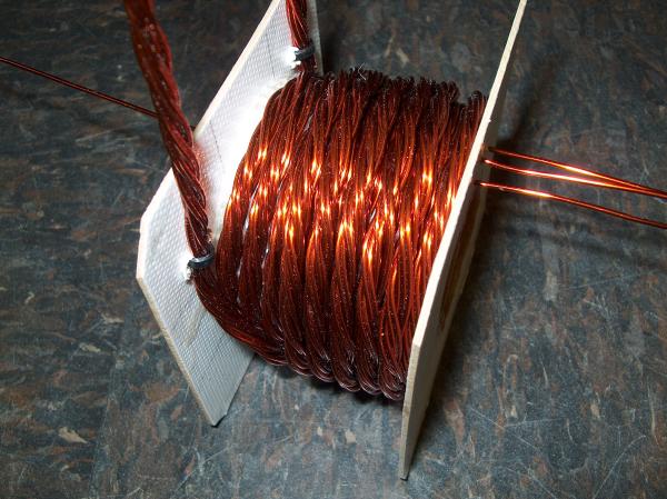
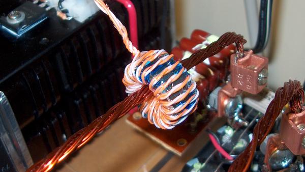
#8 or #10 AWG Litz wire would be ideal for the primary winding, but simply using multiple parallel strands of thin wire will be quite adequate. 8 parallel strands of # 18 AWG wire works well. I twisted the parallel wires into a pseudo-Litz arrangement, but I am not sure if the results are any better than simply winding the wires in parallel. In a pinch, ordinary THHN plastic covered solid # 10 AWG wire also works with slightly greater losses. Since the primary is on the outside, it's easy to make changes to it. A picture of my home brew Litz wire is shown below.
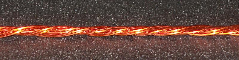
Home brew Litz Wire
The Litz wire was fashioned by taking two parallel strands of #18 AWG wire about 115 feet long and twisting them together in a clockwise direction with an electric drill until the twisted wires had about two turns per inch. The twisted wire was then cut into four equal length and laid side by side. Using the electric drill, the wires pairs were all twisted together into one wire bundle, but this time the twist was done in a counterclockwise direction. Twisting was stopped when the finished wire bundle had a twist of about one turn per inch.
The finished Litz wire was then wound over the completed secondary winding and attached to the coil form sides using plastic tie-wraps threaded through small holes punched in the sides of the coil forms.
Do not wrap the primary winding too tightly against the secondary - you do not want to crush the secondary winding. Do not use insulating tape over the outside of the finished primary winding. The winding will get fairly warm during operation, and it needs free air circulation to cool it properly.
Be sure to carefully clean and tin each strand of wire with solder. Make sure all the strands at each end of the twisted wire are completely soldered together so that each strand will carry an equal share of the primary current.
Before the final assembly of the transformer, make sure that the mating surfaces of the core sections are parallel, smooth and clean. When placing them together, ensure that the minimum air gap is obtained. You should not be able to see light between the core sections when they are placed against each other.
PRIMARY SNUBBER NETWORK:
All transformers have some leakage inductance, and the effect of this is to cause voltage spikes across the switching transistors. To counteract this, a snubber (damping) network consisting of resistor R4 and capacitor C2 are connected directly across the primary winding of transformer T2. Keep the leads connecting R4 and C2 as short as possible to avoid creating a parasitic resonant circuit across the transformer. If transformer T2 is carefully constructed, the leakage inductance will be minimized, and there will be very little difference seen in the voltage waveform present across transformer T2 with or without the damping network installed.
DC BLOCKING CAPACITOR
Capacitor C1 is used to block any DC component of the pulses from Q1 and Q2 from causing a shift of the operating point on the magnetic hysteresis curve of the ferrite core in transformer T2. A DC component can be the result of a leaky switching transistor, or a problem in the gate drive circuit. If the operating point of the ferrite core shifts excessively, the ferrite core may saturate and excessive current will flow through one of the switching transistors, possibly causing the transistor to fail.
C1 is made from 6 - 2 uF 250 Volt poly film capacitors, for a total capacity of 12 uF. The capacitors were salvaged from old computer power supplies. The exact type of capacitor used here is not critical, as long as the capacitor does not become warm in operation and the waveforms as seen across transformer T2 look correct. (See pictures later in this document.)
C1 has a capacitive reactance of about 0.5 Ohms at the operating frequency of 27 kHz.
HIGH VOLTAGE OUTPUT CIRCUITRY:
The 1,600 VAC is then full wave bridge rectified by a bank of 20 - UF4007 high frequency high voltage diodes and choke input filtered by inductor L1 to 1,500 volts DC. The high voltage filter capacitor C6 is of small capacity (2 - 6 uF) by normal standards, but the small capacity limits the amount of stored energy in the event of an internal amplifier tube arc or a high voltage to earth fault path. Voltage ripple is not a problem because any ripple resulting from the high operating frequency of the switching supply is effectively filtered out by filter capacitor C6, and any 60 or 120 Hz ripple from the mains power is regulated out by the PWM circuitry.
HIGH VOLTAGE RECTIFIER:
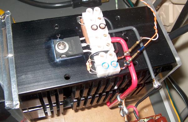
My first try at the high voltage rectifier - 16 - UF4007 diodes in a full-wave bridge configuration.
This arrangement lasted until I started testing at about 1,200 volts and 500 mA load. At that point, all of the diodes in one leg of the bridge shorted and the power supply shut down. I thought this was rather strange, since the voltage rating of each diode was 1,000 volts, and the current rating was 1 ampere. I had individually tested each diode before assembly and verified that each one would handle at least 1,000 volts before breaking down. I also had noted that the diodes became pretty warm - well, quite hot, to be exact - while in operation.
The Second High Voltage rectifier.
Back to the drawing board. I suspected that the cause of the failure might be a voltage spike, so a second bridge rectifier was constructed.
For my second try at making a bridge rectifier, I used a total of 20 - UF4007 diodes, 5 diodes per bridge leg. I assembled the bridge between a pair of screw-type terminal strips. This made it much easier to replace a diode should one fail, and also made making connections to the rectifier assembly very easy.
I also left the leads of each diode full-length for cooling, since, according to the diode manufacturer, most of the heat is removed from the body of the diode through the leads. Figuring that the copper leads were a fairly good heat sink, I bent the diode leads in a zigzag shape so that when the bridge was placed in an upright position, cooling air would be able to freely flow between and around each diode lead for the best cooling effect.
Although this bridge rectifier seemed to work correctly, it still got rather hot. I investigated and found that the losses were not what I had expected. At 60 Hz, where most of us have had power supply experience, most of the loss in a solid state diode is simply the I^R loss in the diode when it is conducting in the forward direction. At high frequencies, however, things are quite a bit different. There is another loss component in a semiconductor device such as a diode, and that is the losses that occur when the device turns on and again when it turns off.
Each semiconductor device has a fairly constant time which is required for the device to turn on and turn off. During the transition periods, the device resistance is higher than when it is turned completely on, and so during the transition time the I^R losses are quite high. This time is quite short, usually in the range of 25 - 100 nanoseconds. The thermal energy created during these transition times are averaged out in the physical mass of the diode and appears as part of the temperature rise during operation.
At 60 Hz, the total of the transition times per second is very low, but at 27,000 Hz where this power supply operates, the total of the transition times per second is 450 times larger. This causes the total transition time losses to increase by 450 times, which causes the diode to experience a considerable increase in temperature when operated at 27,000 Hz.
There's something else to consider, too. I found that if I operated the power supply at 1,000 volts at 500 mA, the diode bridge got quite a bit hotter than it did if I operated the power supply at 1,500 volts at 500 mA. At first, this did not appear to make sense, but then I remembered that the voltage drop across a diode increases in a non-linear manner as the current through the diode increases. But the power supply is supplying the same current to the load in both cases even though the voltage is different. And the current has to pass through the diodes, so what's happening?
When the power supply is running at 1,000 volts output, the switching transistors Q1, Q2 are turned on for less time than they are when the supply if producing 1,500 volts output. (A lower output voltage or current means a shorter switching time.) At first glance it would seem that the diodes should run cooler at 1,000 volts, since they are carrying current for a shorter time each cycle. But, the transistors supply current in pulses, and those pulses are smoothed out by choke L1 to produce the average 500 mA output current. Although the diodes are conducting for a shorter length of time, they are carrying a higher current during that time. There has to be enough current supplied to the rectifier diodes in each switching pulse so that when the pulses are smoothed out by the filter network, the average power will be correct. Because the voltage the transistors switch into the transformer is fixed at +/- 130 volts, the current supplied to the filter network must be greater if the switching pulse is narrower but the load current remains the same. (Trust me; it works that way.) Since the diode I^R losses rise disproportionately as the current increases, the diodes can overheat at what appears to be a safe current level.
The Third Time's The Charm.
The fix turned out to be simple; just parallel another set of diodes with the first set, as shown in this picture. This works without any balancing resistors in series with the diode strings because if any string of diodes carries more current than the other parallel string, the higher current will cause a greater voltage drop across that diode string, causing the other diode string to automatically increase its conduction, thereby tending to equalize the current flow through the parallel diode strings.
HIGH VOLTAGE FILTER:
Smoothing Inductor L1 ready for installation.
Now that the 1,600 volts AC has been converted into pulsating DC, it will be filtered into pure DC by inductor L1, and capacitor C6, which is not shown here. The filter network is a choke input filter. Do not use a filter capacitor on the input of the L1. A capacitor in that position will behave as a short circuit between the output of the bridge rectifier and ground . This will cause the supply to immediately shut down due to excessive switching transformer current.
Choke inductor L1 was constructed from an old LOPT (horizontal flyback transformer). All the windings were stripped from the core and a new coil form was constructed to fit the core much in the same manner as was done for switching transformer T2. The core of L1 is about 1 cm^2. in cross-section, and is probably made from #43 or #77 material. Whatever it is, the material is acceptable for our purpose, since the power supply operates in the same frequency range as the LOPT originally used.
The finished choke coil and the two halves of the ferrite core.
After constructing the coil bobbin, it was wound with about 245 turns of # 21 AWG enameled wire, close wound. Each layer was covered with two layers of insulating tape, and the next layer was wound in place. No special winding method was used; the winding layers were simply wound back and forth until the required number of turns were wound.
Using the power supply design formulas which are found in the ARRL's Radio Amateur Handbook, the critical minimum inductance required for proper filtering was calculated to be close to 9 mHy. Less inductance would fall below the critical value of inductance at the minimum design load current of 75 mA, possibly causing voltage regulation problems. When it was finished and tested, inductor L1 had an inductance of 56 mHy with both of the the ferrite core sections in place and no air gap between the core sections.
I knew that it would be necessary to provide a small air gap between the ferrite core sections in the finished inductor to prevent core saturation when the inductor was carrying 750 mA at full load. That meant that the inductance of the finished coil would have to be greater with the core sections in place and no air gap between them. Some rewinding was required to determine the correct number of turns for the completed coil.
Inserting two thicknesses of a business card between the opposing ends of both sides of the two core sections was sufficient to reduce the inductance to 11.6 mHy after the core sections were placed against each other inside in the coil. This was above the critical inductance of 9 mHy, so I knew that the choke inductor would work properly. Higher inductance than the minimum required is good, less is not good. One of the two air gaps is seen in the picture below and is visible as the thin white line in the center of the right hand core leg. The other gap is hidden inside the center of the coil form.
The exact number of turns and the spacing of the air gap will need to be adjusted in your unit, and will depend on the type of core material and size of core you have available. The picture below shows the finished coil with the ferrite core sections inserted into the coil form.
Core sections inserted into the finished coil. Note the paper spacers between the core sections.
Side view of the completed choke coil L1.
DAMPING NETWORK:
When a voltage square wave is applied across an inductor, as is the case when the high voltage bridge rectifier diodes begin conducting at the beginning of each power switching pulse, the voltage charges the self-capacity of the coil. This causes the inductor and its self-capacity (which form a parallel resonant circuit) to begin a damped oscillation, in much the same manner as a bell rings when struck by a hammer.
This transient oscillation also causes the current flowing through the inductor to oscillate as well. This ringing is also reflected back into the current waveform in the primary and secondary windings of T2. This ringing will make the current supplied by the switching transistors during each switching pulse very irregular, possibly exceeding the maximum allowable current the transistors can handle. Under severe ringing conditions, the current flow will actually try to reverse and flow backwards from transformer T2 into transistors Q1 and Q2. Diodes D3 and D4 will attempt to clamp this reverse voltage. This will cause excessive current to flow through transformers T2 and T3, triggering the automatic shutdown circuit.
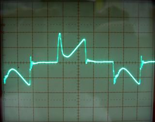
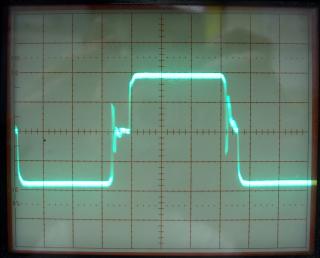
No damping network across L1. (Full power)
This is what the current waveform through T2 and L1 looks like with no damping network installed across L1. In this picture, the power supply is running at full load. Notice that after the current rises to the maximum on the first half cycle, it swings negative towards zero (at the middle line on the oscilloscope screen). If it were to go below zero to a negative value, it would cause one of the diodes across the switching transistors to conduct, triggering an overload shutdown. A damping network must be installed to suppress this severe ringing. The damping network is composed of resistor R5 and capacitor C5.
Optimum value damping network across L1. (Full power)
Here you see the difference in the current waveform when the correct damping network has been connected across L1. In this picture, the power supply is running at full load. The first half cycle of the oscillation is still present. It will be there, because this represents the current necessary to charge the self capacity of the inductor. But notice that the remainder of the waveform has been modified so that all that remains of the damped oscillation which was visible in the first picture is just a smoothly rising waveform. Except for the capacity charging half cycle, this is pretty much the classical trapezoidal waveshape you see for current flowing through an inductor when the inductor has a square wave voltage applied across it.
NOTE: If you tweak the damper network values, you can get the current waveform to become an almost perfect square wave, however, this is incorrect, and is not what you want to happen. What will happen is that the damper resistor will get very hot, since it is dissipating the extra power represented by the area under the curve which was "filled in" by changing the current waveform from a trapezoid to a square wave. You will also find that the mains power required by the power supply will increase, indicating that extra power is going somewhere. It is - but not to the load - it's all going to heat the damper resistor.

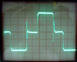
Optimum damping network across L1. (Half power)
Dropping the load on the power supply to about half power results in the average current decreasing during the switching pulses. The pulse length is also shorter, indicating that the transistors are supplying less power to the switching transformer. Note that the initial charging current still peaks at about the same height as it did at full load. This is because the pulses, although of shorter time length, are the same voltage level at half load and at full load. In fact, the voltage will be the same at any load.
Optimum damping network across L1. (One-quarter power)
In this picture, the power supply is running at one-quarter load. The pulse length is shorter still, and the average current is also slightly less. This waveform is pretty much what you should see when the damping network components are correctly chosen.
To determine the optimum values of the damping network components, a couple of "rules of thumb" are:
1) The lower the resistance of R5, the flatter the waveform will be - but the losses will also be larger - so keep R5 as high resistance as possible.
2) The greater the capacity of C5, the more damping effect it will have on the first cycle of the ringing. Note that too low a value of R5 will cause C5 to form a parallel resonant circuit with L1 and make the ringing worse. Too small a value of C5 makes R5 ineffective at changing the slope of the waveform. C5 should be as small as possible while still removing most of the oscillation from the waveform, except for the first half cycle.
You may also obtain a close approximation of the correct values by using the following formulas:
Calculate the XL of L5 at (2 * Switching Frequency)
XC of C5 = (2 * XL)
R5 = XL
In this case:
L5 = 10 mHy
(2 * Switching Frequency) = 54,000 Hz
Using the Reactance Chart in the ARRL Handbook we find that:
XL = 2,500 Ohms
XC = 5,000 Ohms, or about 600 pF
R = 2,500 Ohms
The power rating of R5 must be determined experimentally. If it burns up, it was too low a wattage.
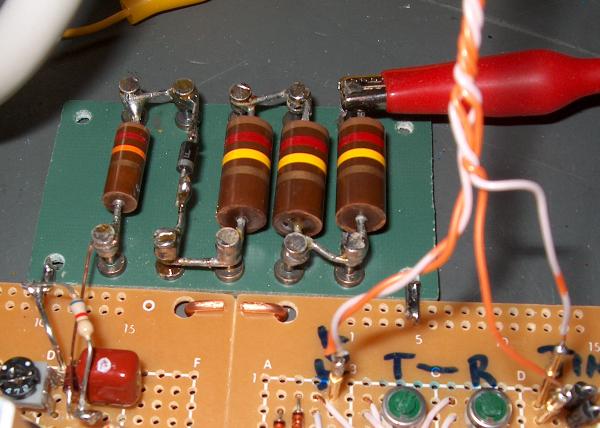
Switching transformer, high voltage rectifier and filter, and damping network.
The picture shows the switching transformer, which is connected with the white clip leads to the high voltage bridge rectifier. The rectifier assembly is mounted on the frame of choke L1. Beneath L1 are the high voltage capacitors which make up C6. The large brown power resistor is the damping resistor R5, and the brown cased Mica capacitor connected to R5 is snubber capacitor C5. Capacitor C6 is an ordinary oil-filled metal-film paper capacitor. I used several high voltage capacitors salvaged from old microwave ovens. These were placed in parallel to obtain the required capacity.
PWM CONTROLLER AND REGULATOR:
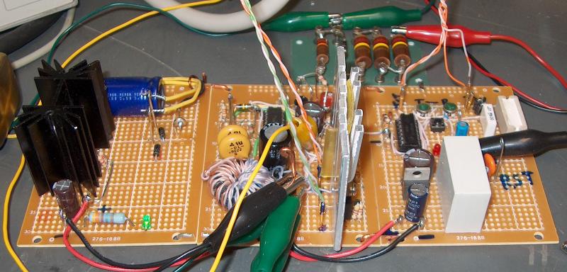
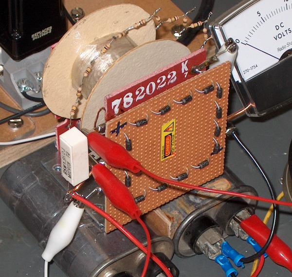
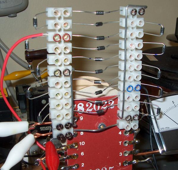
The Pulse Width Modulator and Safety Logic assembly, with power supply.
To regulate the power supply's output voltage, pulse width modulation (PWM) controller U1 samples the rectified and filtered 1,500 volt output of the supply and compares it to a stable reference voltage. As either the mains voltage or the connected load changes, the PWM controller adjusts the pulse width (also called the "duty cycle") of the gate drive signal sent to the main switching transistors Q1, Q2. This variation in pulse width turns the switching transistors on and off for varying durations, so that the DC output of the power supply always matches U1's internal reference voltage. This causes the output of the power supply to remain very close to the set point of 1,500 volts (or whatever you have set it for.) A special high voltage Zener diode, ZD2, with approximately 1,000 volts rating is used in the voltage regulation feedback circuit to improve the voltage regulation. This is an optional component, but the voltage regulation is somewhat poorer without it.
DETAILED PWM CIRCUIT DESCRIPTION:
The PWM circuit consists of IC U1, which does the actual pulse width control and voltage regulation functions, and IC U3 which serves as the control logic for the safety shutdown system. Because the PWM and safety circuits must be ready at all times, they are operated from a separate power supply transformer.
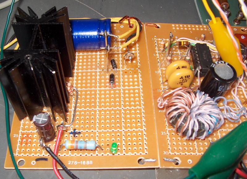
Power transformer T4 supplies 24 VAC center tapped which is full wave rectified by diodes D45 and D46 and filtered into +18 VDC by filter capacitor C12. Three-terminal adjustable voltage regulator U2 is trimmed by resistors R21 and R22 to regulate the +18 VDC down to +10.5 VDC. The +5 VDC is used to operate PWM IC U1. U2 is attached to a heat sink. Capacitor C11 serves as the output filter capacitor for the +10.5 volts produced by U2. Both capacitors C12 and C11 must be placed close to U2 to prevent possible oscillation in the +10.5 volt buss. LED D47 and current limiting resistor R23 are used to indicate the presence of the +10.5 VDC power. These are optional components.
Note that 10.5 volts is used instead of something more "normal" such as 12 or 15 volts. This is because U1 cannot handle a higher voltage than 10.5 without overheating when it is operating at maximum pulse width. This is because it must supply several watts of gate drive power to the driver circuits for the IGBT switching transistors.
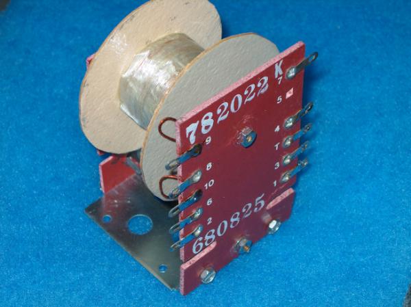
Left - Power Supply, right - PWM controller U1 and transformer T1
Power for U3 is supplied by fixed +5 volt regulator U4. Because of the low current required by U3, no heat sink is needed for U4. Capacitor C15 is the input filter capacitor for voltage regulator U4 and capacitor C16 is the output filter capacitor. . Both capacitors C15 and C16 must be placed close to U2 to prevent possible oscillation in the +10.5 volt buss.
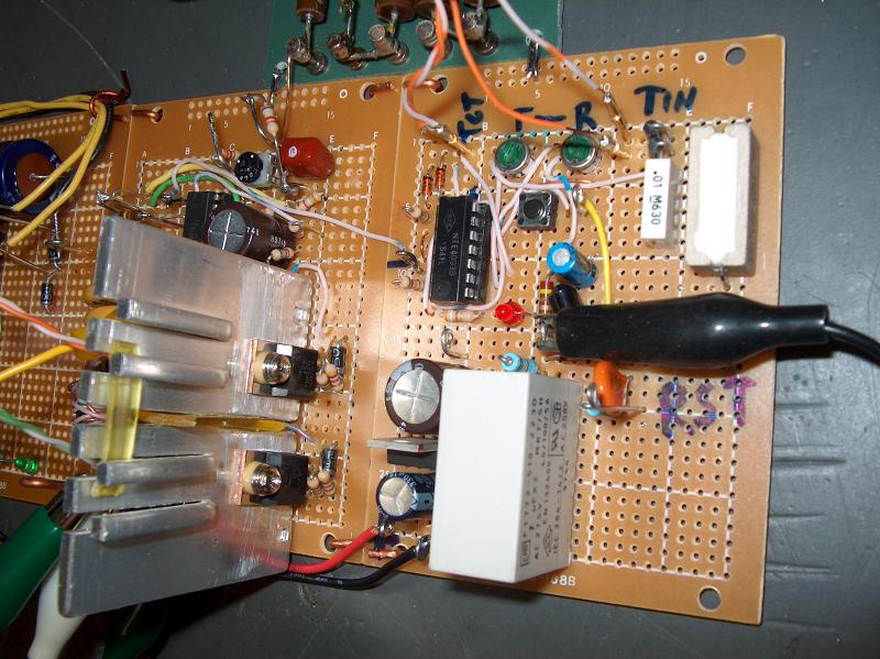
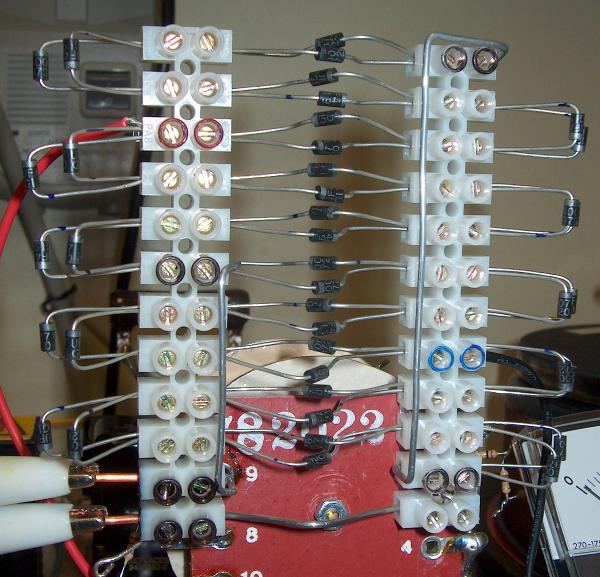
Right-hand board - Safety Shutdown circuits, left-hand board - PWM controller and transistor drivers Q3 and Q4 seen here mounted on their aluminum heat sinks.
PWM IC U1 generates an internal sawtooth wave at 54 KHz, which is twice the switching frequency of 27 KHz. The sawtooth frequency is determined by the values of R15 and C8. This sawtooth is used as one of the inputs to a pair of internal voltage comparators, one of which monitors a voltage sample from the +1,500 volt line, and the other, which looks at the output of the safety shutdown circuit, U3. Filter capacitor C9 must be placed close to U1 and connected with short leads to prevent possible unwanted oscillations.
An internal +5 VDC reference voltage is generated on pin 14 of U1. This is divided by resistors R24 and R25 to create a +2.5 VDC reference signal. The +2.5 VDC reference is sent to the - input of both of the internal comparators on pins 2 and 15.
Pin 3 is a compensation feedback output signal, which is mixed with the +2.5 VDC using resistors R13 and R12. This reduces the gain of the comparators from 80 dB to about 16 dB. This is sufficient gain for the regulator to function properly, but not enough gain to cause unwanted feedback and circuit oscillation.
To make sure the power supply has a "soft" start-up, capacitor C17 and resistors R31, R32 and R33 provide a controlled voltage ramp on U1 pin 4 that falls from about +4 volts to zero about three seconds after relay contact K1b closes. R14 helps keep stray noise out of pin 4. This falling waveform allows the pulse width signal which is sent to the switching transistors to gradually increase in width over the three second start up interval, and this gradually brings the output of the power supply up to full power over three seconds. Opening relay contacts K1b allows capacitor C15 to recharge within about 1/2 second, and rapidly brings the power supply's output down to about 10%.
PWM OUTPUT DRIVER CIRCUIT
After the pulse width modulated switching drive pulses have been generated by U1, they are used to drive the gates of transistors Q1 and Q2. The base of commonly used bipolar transistors present a mostly resistive load to the driving circuit, but IGBT's are quite different. Just like a MOSFET, IGBT's present a very high resistance load to the driving circuits, and, also like a MOSFET, they present a fairly large capacitive load to the driver.
For all practical purposes, the gate of an IGBT is a capacitor. This makes the gate drive circuitry somewhat more complicated than it would be if we were using bipolar transistors. To add to the complications, the operating characteristics of U1 also affect the required drive circuitry.
If you look at the diagram of the driver circuit between the output of U1 and the gates of the IGBT's, you will see that the circuit is a moderately complex push-pull drive system. Let's analyze it in detail.
The first thing to notice is that the secondary side of T1 has two identical windings. Each winding is used to drive a separate IGBT. Separate windings are used because the emitter of Q2 is at -130 volts, and the emitter of Q1 is at either + or -130 volts, depending on whether Q1 is on or off. This makes a common reference connection for both IGBT's impossible, and so we need separate drive windings on T1.
The primary of T1 is center tapped, with the center point of the winding connected to the +10.5 V power buss. Each end of the primary winding is connected to its respective output connection from U1. The output stage in U1 is capable of supplying 2.5 watts of power through T1. Each of the output transistors in U1 provides one of the two switching drive pulses to the primary of T1, and they are combined on both of the secondary windings of T1 and appear as a 27 KHz AC waveform. The waveform appears as a series of alternating positive and negative pulses of variable width.
Notice that the relative polarities of the two secondary windings is reversed, so that when the top of winding 1 is positive with respect to the bottom of winding 1, the top of winding 2 is negative with respect to the bottom of winding 2. This is because the transistors must be turned on alternately, but never both at once, or a short circuit would be placed directly between the + and -130 volt busses.
Now, you might ask just why do we need all of those other components between the secondaries of T1 and the IGBT's? After all, we could just connect one end of the secondary winding to the emitter of each transistor and the other end of the secondary winding to the gate lead of the IGBT. That should work, and it would allow each gate to go positive on its own positive drive pulse, and the transistor would ignore the negative pulse - right?
Sorry, that doesn't work. Remember that the gate appears as a capacitor, and a pretty large one, at that. In fact, the transistors used here represent a 7,000 pF capacity. Since that capacity is essentially placed directly across the secondary windings, what happens is that a very effective parallel resonant circuit is formed by the gate capacitance and the secondary windings of T1.
It's important to understand that the output transistors of U1 are only turned on during the switching cycle for the amount of time required to generate the PWM pulse, and during the remainder of the switching cycle they are turned off. During the transistor off time periods, the primary winding of T1 is effectively open circuited, because there is no damping effect from the driver transistors in U1 because they are not conducting. During this off time, the energy which was pumped into the gate capacitance of the IGBT's will oscillate back and forth through the secondary windings of T1, causing the IGBT's to turn on and off following the oscillating gate signal. This causes the system to overload and shut down. We must stop this oscillation from happening.
We can do this by adding a few parts to the circuit. First, we add a pair of diodes, D25 and D26. These allow the positive drive pulses to get to the gates of the IGBT's. Since the diodes do not allow the gate charge to return to the secondary windings when the gate pulse ends, we have stopped the oscillation from happening. Of course, what will happen is the gates will stay charged positive - the gate capacitors are very high quality, and have very low leakage - and as soon as the second transistor turns on, we find that we now have a dead short through the transistors directly across the + and -130 volt buss. Oops! We need to fix that.
We do that by adding a pair of transistors Q3 and Q4 between the gate and the emitter of both of the IGBT's. The purpose of Q3 and Q4 is to dump the charge on the gate of the IGBT's as soon as the positive drive pulse goes away. This will turn the IGBT's off and dissipate the gate charge energy as heat in the transistors ON resistance. That's why transistors Q3 and Q4 are mounted on heat sinks. Now, remember that I mentioned that during the drive pulse off periods that U1's transistors are off and provide no signal to T1? That means that there is no power available on the secondary of T1 to turn on Q3 or Q4. So how do we get these to switch on and dump the gate charge?
Resistors R8 and R9 (on Q3) and resistors R10 and R11 (on Q4) form a voltage divider network arranged so that when the positive gate drive pulse is present, transistors Q3 and Q4 will be turned off. (They are PNP transistors, so making the base positive with respect to the emitter turns the transistor off.) When the gate drive pulse turns off, resistors R9 and R11 pull the bases of Q3 and Q4 towards the collector voltage, turning Q3 and Q4 on and dumping the positive gate charge which was put into Q1 and Q2
Resistors R2 and R3 are used to prevent leading edge ringing on the gate drive signal caused by the rapid rise of current through the wire connecting to the gate of the IGBT's.
It requires about +5 to +8 volts to turn the IGBT's on. They can tolerate as much as +30 volts on the gates, and +15 volts is recommended by the manufacturer. Transformer T1 provides about 15 volts on each secondary winding, but a volt or so is lost in the driver circuitry. Using a higher voltage would improve the IGBT rise time slightly, but would involve adding an additional set of driver transistors because the output stage in U1 cannot handle any additional output power.
The next two pictures show the waveforms you should see if you connect your oscilloscope probes across the secondary windings of driver transformer T1.
SAFETY WARNING: The circuits you are measuring do not have the same earth reference for the two transformer windings - they are 130 volts different in potential. The oscilloscope probe shields must be connected to the low side of the driver transformer secondary winding which is connected to the emitter of Q2. This means that the case of the oscilloscope will be at -130 volts DC with respect to earth. Ensure that the case and all connections to the oscilloscope are isolated from contact with anything else, including the operator. It is essential that you use an isolation transformer between the mains voltage and the power supply for operator safety when taking these oscilloscope measurements.
DEATH IS PERMANENT
PLEASE BE CAREFUL!!
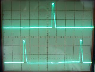
Gate Drive at low power = minimum pulse width
This is what the gate drive pulses to the power IGBT's looks like. Notice the very short ON time. The power supply is running in the first part of the three second soft start cycle.
Gate Drive at high power = maximum pulse width
Now the three second soft start time has elapsed and the power supply is running at full load. Notice that the gate drive pulses have widened out to full width. You will note that they are not quite at a 50/50 on/off ratio. This is because we must allow some time for the transistors to turn off before the next one is turned on. The PWM IC handles this, by limiting the ON time to a maximum of 45%. This means that we must design the switching transformer to work as though it were being supplied with a 50/50 square wave but with only about 90% of the actual voltage we have available in our supply. If we don't remember do this, we will find that the output voltage is about 10 to 15% lower than we expect. This is an interesting "Gotcha'!" in switching power supply design, and catches many beginning designers by surprise.
The next two pictures show the waveforms you should see if you connect your oscilloscope probe across the primary of the switching transformer T2.
SAFETY WARNING: The low side wire from the primary winding of T2 is connected directly to one side of the AC mains. It is essential that you use an isolation transformer between the mains voltage and the power supply for operator safety when taking these oscilloscope measurements.
DEATH IS PERMANENT
PLEASE BE CAREFUL!!
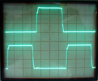
T2 Primary Voltage waveform at low power
Notice that the transistors are conducting for less than the maximum time available.
T2 Primary Voltage waveform at high power
The transistors are turned on for almost the maximum time the PWM will allow.
High Voltage Sense Resistor string and ZD2
HIGH VOLTAGE REGULATION
To accomplish the voltage regulation of the power supply, a voltage sample is taken from the +1,500 volt line through resistors R17, R18, R19, and R20, and Zener diode ZD2. This voltage sample is sent to U1 pin 16. Adjustment of the power supply output voltage set point is done with potentiometer VR1. The span and range of the voltage adjustment set point are set by selecting R34 and R16. Zener diode ZD1 is a protection diode for U1 in case of a failure of voltage dropping resistors R17, R18, and R19, or in case ZD2 shorts out.
Three two-watt resistors placed in series are used for the voltage dropping resistor string of R17, R18, and R19. Multiple series resistors are used to avoid an excessive amount of voltage from being placed across any one resistor with the chance of a catastrophic high voltage flashover. R20 is optional, and its resistance may be included anywhere in the voltage dropping resistor string. It was placed in the position shown in the diagram to allow me to obtain a sample of the feedback voltage reading during testing.
Zener diode ZD2 requires special mention. 1KV Zener diodes are not commonly stocked by your friendly local parts supplier. So, we shall "roll our own." But, why do we need to use a Zener diode in this voltage divider network anyway, and even if we do, why is such a high voltage required?
It has to do with the quality of voltage regulation we can expect from the power supply. To maintain a constant output voltage, U1 compares the sample voltage from the power supply output to U1's internal reference voltage. The reference we are comparing against is 2.5 volts, which is 600 times smaller. This means that for the smallest voltage change U1 sees as an error signal and can use to regulate with, the voltage change on the output of the power supply must be 600 times larger. For example, if U1 can hold the voltage to within +/- 0.1 volts compared to the reference, than the output of the power supply can change as much as 120 volts and still be within acceptable limits.
If we were suddenly able to "throw away" or "subtract" a large part of the 1,500 volts DC but still keep the output voltage variation and then send that to U1, we would obtain much better regulation. In this switcher, I have used a 1,000 volt Zener diode to "subtract" 1,000 volts from the 1,500 volts. Now, we see that the 1,500 / 2.5 = 600 in our first example has become (1,500 - 1,000) / 2.5 = 500 / 2.5 = 200, or three times less than the first example. We have just improved the voltage regulation of the power supply from 120 volts to 40 volts, or a three-fold measure of improvement by adding one component.
In this power supply, the regulation of U1 is much better than assumed here, and the actual regulation range in this circuit is closer to +/- 0.01 volts.
You can "build your own" Zener diode by carefully reverse biasing common 1N4007 diodes from a high voltage source through a high value resistor - 10 Meg Ohms or so - and measuring the voltage at which the diode begins to conduct in the reverse direction. The best diode will have a "hard" clamping voltage, i.e., the Zener voltage will change very little as the current through the diode varies.
For a PDF file showing the simple test setup needed to determine the Zener voltage of reverse-connected high voltage diodes, please click HERE.
OVERLOAD SAFETY CIRCUITS:
Safety against overloads is provided in the form of load over current detection, and switching transistor overcurrent detection. The protection circuits are fast enough to shut down the power supply within less than 1/2 of one switching cycle in the event an overload is detected. The power supply must be reset from an overload manually.
The safety shutdown circuit consists of IC U3 and associated components. The heart of the circuit is the flip-flop composed of U3c and U3d. Resistors R27 and R28 provide input pull-up voltage to flip-flop pins 1 and 6. To ensure that the flip-flop comes up in the correct state at power on time, capacitor C7 and resistor R35 provide a power on time delay low-to-high transition which holds pin 6 of U3d low long enough for the flip-flop to start up in the correct state.
A high to low signal from either U3a or U3b will be gated through diodes D50 and D51 to pin 1 of U3c. This low will cause the flip-flop to change states, and forcing U3d to go low, lighting LED D54 which indicates to the operator that an overload event has happened. At the same time, pin 3 of U3c will go high, setting pin 1 of U1 high, turning off U1, which removes the gate drive from switching transistors Q1 and Q2, effectively turning off the power supply.
RECOVERY FROM AN OVERLOAD - Method 1
If the power supply is wired so that power to the PWM circuits is turned OFF when switch S1 is opened, then the power supply must be reset from an overload by:
1) Shut off the mains voltage by opening switch S1.
2) Wait about 30 seconds for the 130 volt capacitors to discharge.
3) Close S1 to restore the mains power.
RECOVERY FROM AN OVERLOAD - Method 2
If the power supply to the PWM circuits remains ON when switch S1 is opened, then the power supply may be reset from an overload by:
1) Shut off the mains voltage by opening switch S1.
2) Wait about at least 10 seconds for the 130 volt capacitors to partially discharge.
3) Press the Overload Reset switch and release it. (The overload LED should go out.)
34 Close S1 to restore the mains power.
Note that shutting off the power to the PWM circuit automatically resets the overload flip-flop. If the PWM power remains on, then pressing the manual reset button is required. Using the manual reset could potentially be damaging to the power supply should there be a shorted switching transistor. The manual reset circuit prevents "jamming" of the reset circuit by holding down the reset button and attempting to force the power supply to restart in the event an overload still exists.
OPERATION OF THE MANUAL RESET CIRCUIT
One plate of capacitor C18 is held at +5 volts by R28, and the other plate is also held at +5 volts by resistor R34. This means that C18 is effectively discharged. When the overload reset switch is pressed, one side of C18 is pulled low. This forces the other side of C18, which is connected to U3d pin 6, to be pulled low, resetting the overload safety flip-flop U3c and U3d. This low remains on U3d pin 6 until C18 charges.
The time required for C18 to recharge through R28 is less than 10 microseconds. This ensures that the reset pulse "goes away" very quickly so that the flip-flop can be tripped again if an overload still exists. In other words, the reset pulse ends so fast that before the next power on switch pulse from the switching transistors is more than half done, the flip-flop can shut down the transistor that is trying to turn on again, thereby saving things from a catastrophic failure.
Switching Transistor Over Current Sample Transformer T3
PROTECTION AGAINST SWITCHING TRANSISTOR OVERLOAD
Transformer T3 is used to protect the supply from overloads caused by excessive current through the primary of T2, and also to shut down the supply in the event of a shorted IGBT transistor.
One lead of the primary winding of switching transformer T2 makes a single pass through T3. This single pass forms the primary winding of T3. This means that any current flowing in the primary winding of transformer T2 will induce a voltage into the center tapped secondary winding of T3. This voltage, which represents the current flowing through the primary of T2 appears across load resistor R26 and is full wave rectified by diodes D48 and D49. Because the signal is at 27 KHz, type UF4007 diodes are used. The rectified DC signal is filtered by C13 and appears across potentiometer VR2.
WARNING: Resistor R26 MUST be connected across the secondary winding of T3 at all times. This is because T3 is a current transformer. If the secondary of a current transformer is not connected to a load (that is, if it is "unburdened") the voltage across the open secondary winding may reach very high values, even to the point of arcing. In addition, the impedance of the primary winding of the current transformer (one turn, in this case) will increase greatly, resulting in a drastic fall-off in power through the system. In this power supply, removing R26 during testing resulted in the output voltage of the power supply dropping from 1,000 volts to less than 200 volts. No attempt was made to measure the voltage appearing across the secondary of T3.
If the current through transformer T2 increases sufficiently, the voltage at the gate of IC U3B pins 8 and 9 will go high enough to force the output on pin 10 low. The low will be gated through diode D51 to U3c pin 1, pulling it low. This will force U3c pin 3 high, and set the U3c-U3d flip-flop to the shutdown state. Potentiometer VR2 is normally adjusted to cause shutdown of the power supply at about 15 amperes peak transformer current.
PROTECTION AGAINST A SHORTED SWITCHING TRANSISTOR
From inspection of the diagram, you can easily see how sample transformer T3 will monitor the current flowing from switching transistors Q1 and Q2 to the switching transformer T2, thereby protecting against overcurrent through the transformer. But what about the case where either Q1 or Q2 fails shorted? Since transformer T3 does not "see" current flowing directly between Q1 and Q2, what will happen if one of them shorts out?
Interestingly enough, it turns out that T3 handles that, too. Here's how it works. Remember capacitor C1? It blocks any DC from getting into the primary winding of T2. Because of the large value (12 uF) of C1, during normal operation C1 never has a chance to charge up very much before the opposite polarity switching pulse arrives and discharges C1. This means that C1 normally has little, if any, DC voltage charge.
Now, suppose that Q1 has failed and become a dead short circuit. This means that +130 volts will be steadily applied to capacitor C1 through now-shorted transistor Q1. Since C1 is now connected to the +130 volt buss for a much longer time than normal due to the short through Q1, capacitor C1 will be able to charge to a higher DC voltage than it is supposed to in normal operation. C1 will continue to accept a DC charge through Q1 until Q2 is turned on by the driver circuit of U1.
As soon as Q2 turns on, there will be a short circuit formed between the +130 and -130 volt buss through transistors Q1 and Q2. At that instant, the side of capacitor C1 which was at +130 volts is suddenly lowered to zero. (+130 volts through shorted transistor Q1 plus the -130 volts through just-turned-on transistor Q2 equals zero volts at capacitor C1.)
C1 immediately starts to fall back to zero volts. Because C1 has been charged to a higher than normal DC voltage by virtue of shorted transistor Q1, the current flowing from C1 and through the primary winding of T2 will be much greater than normal. Transformer T3 will detect the excessive current and cause the overcurrent protection circuit to shut down the power supply.
PROTECTION AGAINST EXTERNAL OVERLOADS
Power supply output overcurrent from such things as tube arcs, flashovers and poking your fingers in the PA circuitry with the plate power on are handled by sensing the voltage drop across resistor R1. All of the current from the power supply to the load flows through R1. Although the voltage drop across R1 does affect the output voltage slightly, it is only about 5 volts at 1 ampere load current. The sample voltage from R1 appears across potentiometer VR3, and is filtered by R29 and C14 to remove high frequency noise. Zener diode ZD3 protects against voltage surges in case of a short circuit across the output of the supply which would cause the voltage across R1 to rise to several hundred volts during the short circuit time.
LOAD STABILITY OF THE POWER SUPPLY
The power supply was tested under load and found to be quite stable with loads ranging from 10 to 100%. To determine the performance of the power supply under transient loads, such as might be encountered during SSB or CW amplifier operation, a series of pulse tests were undertaken.
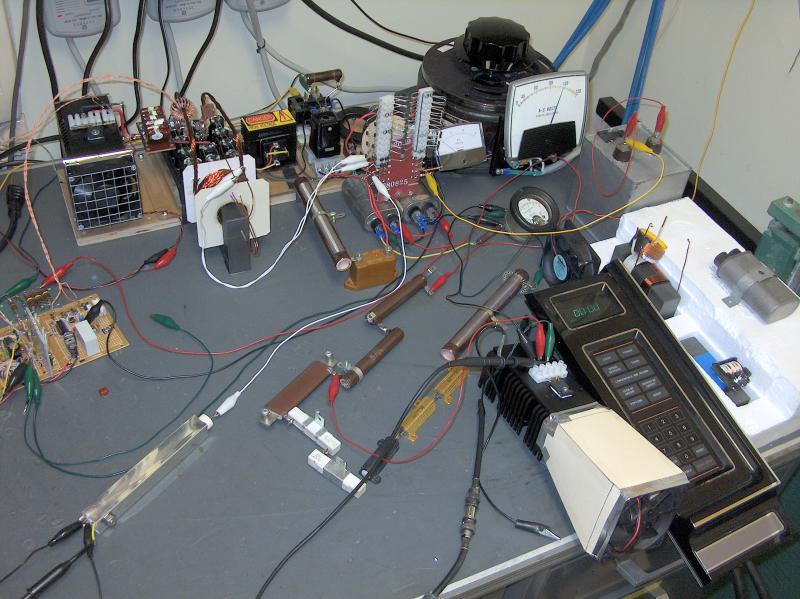
This is the power supply all set up for pulse load testing.
Here you can see the combination of load resistors used for testing. The IGBT transistor which is used to switch the load resistors in and out of the circuit is mounted on the black heat sink with the cardboard fan duct attached to it. Its gate is driven by a function generator. Note the use of a recycled timer panel from an old microwave oven. This makes it very easy to turn the mains power to the switching power supply on for a predetermined length of time for testing. The panel may be moved back a safe distance from the device being tested in case you expect a few parts to explode! The 100:1 high voltage probe is the length of square aluminum tube just to the left of the load resistors.
Using a high voltage IGBT of the same type as is used for the switching transistors, and using a series string of load resistors the test setup was configured so that by gating the IGBT on and off, the current drawn from the power supply could be instantly switched between 175 and 750 mA and then just as quickly switched back from 750 to 175 mA. Using a square wave, the IGBT was gated at various frequencies and for varying pulse widths from 1% to 99% on- to-off ratios. In all cases it was found that the supply operated consistently well, with no evidence of instability or erratic operation.
The pictures shown here were taken with a 100:1 shielded resistive voltage divider network connected across the +1,500 volt output of the power supply. The scale of these pictures is 1 volt per major vertical division.
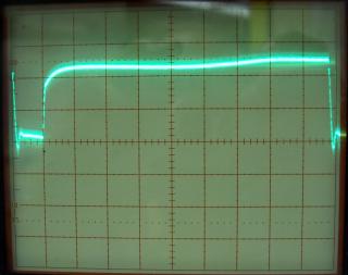
Picture 1) The load pulse is 10 milliseconds per major horizontal division, high voltage filter capacitor is 2 uF.
The output voltage drops by about 2 volts with the application of the load to the supply. It promptly recovers and stabilizes at about than 2 volts below the initial value. At the end of the load pulse, the output voltage rapidly recovers to the previous level. Note the lack of voltage overshoot when the load is removed. The overall shape of the voltage drop and recovery remained the same, regardless of the width of the load pulse.
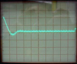
Picture 2) The load pulse is 1 millisecond per major horizontal division, high voltage filter capacitor is 2 uF.
This is the same load pulse as was seen in picture 1, but the horizontal scale has been expanded 10X . This shows that within about 2.2 milliseconds the power supply output voltage has stabilized, with only a very slight voltage undershoot when the load is applied. This appears to be a critically damped wave, which indicates that we should use a filter capacity value of between 2 and 4 uF for good filtering and to limit the amount of stored energy in the filter capacitor in case of an arc in one of the final amplifier tubes.
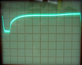
Picture 3) The load pulse is 10 milliseconds per major horizontal division, high voltage filter capacitor is 6 uF.
Here, we have increased the high voltage filter capacitor from 2 uF to 6 uF. The first thing we notice is that the slight voltage undershoot is gone. It also takes a little more time for the voltage to fall to the new, slightly lower value under load. We also see that the voltage recovery time when the load is removed is also increased. It appears that 6 uF is slightly more filtering capacitance than is needed. The waveform is slightly overdamped. There is also more of a "bobble" in the voltage recovery after the load pulse is removed. However, it will work quite well as a filter capacitor in the power supply. One drawback of the additional filter capacity is that with the extra energy stored in the 6 uF filter capacitor, there is more energy available to cause damage should there happen to be an arc in one of the amplifier tubes.
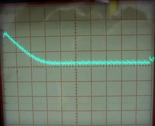
Picture 4) The load pulse is 1 millisecond per major horizontal division, high voltage filter capacitor is 6 uF.
When we look at the load pulse at the same scale as picture 2, we can easily see the absence of the voltage undershoot. Note that it also requires about 3 milliseconds for the voltage to reach its lowest value when the load is applied. This is because of the additional damping provided by the added filter capacity.
CLOSING COMMENTS
It should be mentioned here that the photographs shown here are of the prototype unit. Most of the components will be mounted inside the Heath Warrior amplifier cabinet in place of the original and now defunct power supply. The parts layout on the perf board as seen here is not to be taken as "the last word" in assembly or parts placement. As long as you keep the component leads short and observe good engineering methods, you should have no problems in making this, or a similar switching supply function properly.
I hope this article proves useful to you. Please let me know if you have any suggestions or comments about this article.
73,
W5JGV
Permission to repost or reuse this article on other web sites is available on request. Links to this web site, page, or article are permitted.
All Pages, photographs, text or other data in any form on this Web Site are Copyright © 2004 by Ralph M. Hartwell II.