First Posted December 7, 2011
Revised January 25, 2012 and January 2, 2013 to correct schematic errors and parts values.
By Ralph M. Hartwell, W5JGV
This document describes a Rife Beam-Ray system which was designed and constructed using the latest information available about Royal Rife's actual frequencies.
This system uses a novel method of generating the proper modulation frequency for the 3.1 MHz carrier, and describes the design and operation of the control circuit logic required for that purpose. A method of coupling the power RF amplifier to the Rife Tube that eliminates the commonly used antenna tuner is described. Schematics and construction data are also provided.
Since 1997 I have constructed several different types of Rife Beam-Ray systems. The earlier versions operated on the Bare-Rife principle, where a 27 MHz carrier was square-wave modulated by a sequential series of audio frequency signals. After reviewing the currently available data from many researchers and experimenters, I decided to construct a system which would incorporate the latest frequency data findings as well as some of my own ideas which would allow me to simplify the construction and operation of the system, and make it easier for less technically skilled persons to assemble such a system.
The first task was to determine exactly which carrier and modulation frequencies would likely be the most useful. Please refer to the following documents that are located on the web site, http://www.rifevideos.com .
The pertinent documents are: http://www.rifevideos.com/the_rife_machine_report.html for the how any why of it all. This page allows you to read each chapter on-line. If you prefer, the entire document may be downloaded as a large PDF file at: http://rifevideos.com/pdf/a_history/the_rife_machine_report_a_history_of_rifes_instruments_and_frequencies.pdf .
http://www.rifevideos.com/dr_rife_and_philip_hoylands_3.3mhz_sweep.html explains the the reasoning behind using a 3.1 or 3.3 MHz carrier.
http://www.rifevideos.com/dr_rifes_true_original_frequencies.html provides a more detailed information about the derivation of the correct frequencies.
Be sure to read Chapter 17, "Summary of the Rife Machine Report," for the latest information on these frequencies before you begin building a Rife Machine.
From the information in the documents above, I decided to construct my system using a 3.1 MHz carrier and a sweep frequency from 25,000 Hz to 500 Hz.
The system has to perform several interrelated operations to be useful. First, it must be capable of generating the correct Rife frequencies. By using a 3.1 MHz carrier combined with a separate 25,000 to 500 Hz square wave modulation frequency, the correct frequencies may be generated. Second, the system must be able to get the frequencies into the biological system. This is done by using a Rife Beam-Ray tube, which may be either a Phanatron as Rife used, or a straight tube, with or without internal electrodes. I decided to use a Phanatron tube for this system.
The general layout of pervious systems has been roughly as follows:
AUDIO GENERATOR ---> RF SOURCE (CB) ---> RF POWER AMPLIFIER ---> ANTENNA TUNER ---> RIFE TUBE
This system follow much the same design, but with a few modifications to make it easier to operate. The often complex and expensive audio/function generator is replaced by a simple frequency which smoothly sweeps from 25,000 Hz down to 500 Hz over a period of roughly four hours, or some other time period as set by the operator. To produce this sweep frequency, a common CD or DVD player or an inexpensive computer with a sound card may be used. These devices simply play back a series of audio files generated by any of a number of programs that are freely available on the Internet. If the audio files are "burned" to a CD, they may be conveniently played back using a CD or DVD player. This greatly reduces the expense of purchasing a precision programmable audio oscillator, although such may be used if desired.
Instead of a modified CB radio, a precision 3.1 MHz crystal controlled oscillator module is used to generate the required carrier frequency. This carrier frequency is then modulated by a square wave that is generated from the sweep frequency. The result of this modulation is a series of square wave bursts of 3.1 MHz energy which is then sent to an RF amplifier. After the modulated signal is boosted to the required power level, 50 to 300 watts, depending on the requirements of the Rife tube, the amplified signal passes through a matching network and then on to the Rife tube.
Because the 3.1 MHz carrier signal is between the Amateur Radio 160 Meter and 80 Meter frequency bands, a standard Amateur Radio RF power amplifier may be used to amplify the 3.1 MHz signal up to the power level required by the Rife tube. Usually, a commercially available antenna tuner is used to match the output of the RF power amplifier to the Rife tube, but I have designed a simpler matching system that reduces coupling losses, lowers cost, and improves the wave shape of the signal that is sent to the Rife tube.
Although generating the 3.1 MHz carrier frequency is straightforward - we can simply use a packaged DIP CMOS oscillator - generating the square wave sweep frequency is not so simple. What we want to modulate the carrier signal with is a square wave. However, CD and DVD players, as well as computer sound systems cannot reproduce a clean square wave over the frequency range we need. What they can do, however, is handle sine waves very well indeed. The problem is that the sampling rate of most computer sound cards and many CD and DVD players limits the reproducible upper frequency limit to somewhere near 21,500 Hz. This is a problem, because we need to be able to play back up to 25,000 Hz (or even higher) for this system to work correctly.
The solution in principle, at least, is easy. All we have to do is to divide the required frequency range of 25,000 to 500 Hz by two to get 12,500 to 250 Hz. That frequency range will record and play back perfectly on our CD or DVD player or on our computer. Then, while playing the divided-by-two frequency signal, somehow we double the frequency back to the original frequency range. Next we have to convert the doubled signal to a square wave. From there on, it's easy. The square wave modulates the 3.1 MHz carrier, then the modulated signal is amplified and sent to the Rife tube.
Simple, isn't it? As it turned out, it was not too difficult to accomplish. I'll explain the process when I talk about the Controller Board a little further down the page. But first, let's take a look at the system block diagram.
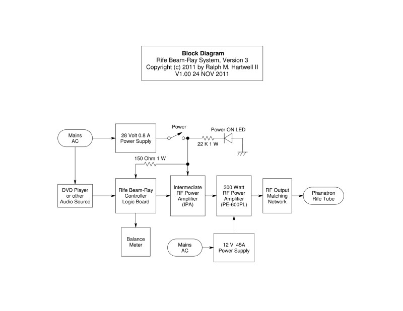
This is the overall block diagram of the completed system. For a PDF copy of this diagram, please click here.
The 28 volt power supply was salvaged from a discarded HP inkjet printer. The modulation signal magic happens in the block marked "Rife Beam-Ray Controller Logic Board." The input to the logic board is a low-level sine wave signal from 12,500 Hz to 250 Hz. The output from the logic board is square wave modulated 3.1 MHz RF at about 800 milliwatts (0.8 Watt) power level. The block marked "IPA" boosts the modulated carrier from the Logic Board to about 10 watts. The 300 watt PE-600PL amplifier was "borrowed" from one of my earlier Bare-Rife systems. Specifications for the PE-600PL amplifier may be found here. This amplifier is no longer available, but several amplifiers from RM Italy, such as the RM-300, and the RM-500, should be acceptable substitutes should you wish to use a solid-state amplifier.
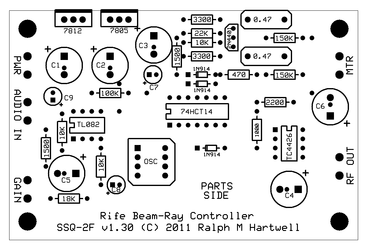
The function of this logic board is to take the divided-by-two frequency sweep from the playback system, double it in frequency, and convert it into a square wave. The square wave then modulates the 3.1 MHz carrier which is generated by an on-board oscillator. Provision is included for adjusting the system audio gain to maintain a consistent square wave. An output is provided for connection of an external meter with which to monitor the symmetry of the square wave. A technical discussion follows the diagram below.
Please click here to download a PDF file of this diagram.
If you want to etch your own double-sided circuit board, please click these links to download a PDF file of the TOP and the BOTTOM of the circuit board.
A drawing of the component placement is HERE.
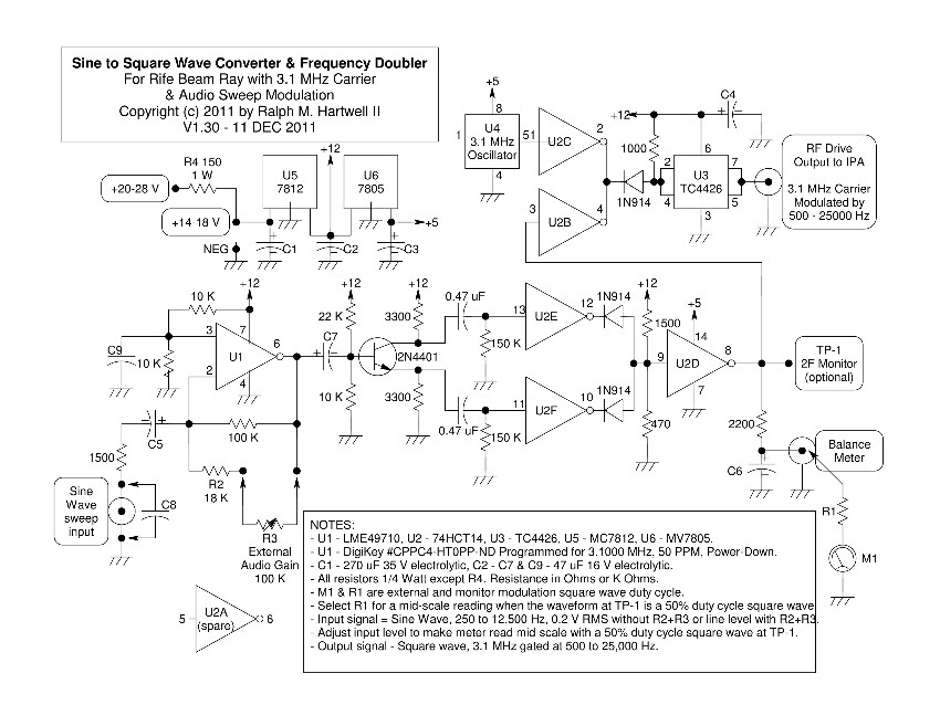
Unregulated DC power is connected to the +14 to 18 Volt input connection. Regulator U5 supplies the +12 volt buss, and regulator U6 supplies the +5 volt buss. Because the power drain of the logic board is low, neither U5 nor U6 require an additional heat sink.
If the logic board is to be powered from a 24 to 28 volt DC power supply, then resistor R4 must be installed to reduce the power dissipation in voltage regulator U5. If resistor R4 is not used with a 24 volt power source, than regulator U5 will require an additional heat sink. Because U6 takes its input power from the regulated +12 volt buss, no heat sink is required on U6.
The sine wave audio signal from the CD or DVD player or computer sound card is applied to the SINE WAVE SWEEP INPUT connector. You will recall that this signal is at one-half the required audio frequency. The audio signal goes to the input of amplifier U1, which has a voltage gain of 10 if R3 is not used. If R3 is used, then the gain will be reduced. R3 is used if the audio signal is derived from a DVD player. This is because most DVD players do not have provision to vary the audio level on the audio output jacks. Without R3, the gain of U1 is higher so that it will accept the signal levels from most computer sound cards.
The amplified sine wave signal from U1 goes to the base of the 2N4401 transistor. This transistor is used as a phase splitter with a voltage gain of 1. The two sine wave output signals are equal in amplitude, but 180 degrees out of phase with each other.
The two 180 degree out-of-phase sine wave signals are sent to U2E and U2F, two gates of a 74HCT14 Schmidt Trigger. This part of the circuit is a bit unusual in that we are using the analog portion of the 74HCT14 input stage to provide level detection. This causes the gate's output signal on pins 12 and 10 to switch on and off as the sine wave input signal passes through the Schmidt Trigger transition voltage level, which is about 2 volts. The Schmidt Trigger function of the gate circuit prevents random jitter and glitches from appearing on the output signal waveform on U2 pins 12 and 10. The resulting output signal from pins 12 and 10 is a clean square wave. The two square waves, like their corresponding input signal sine waves, are also 180 degrees out of phase.
If we adjust the level of the audio frequency input to U1 (or the gain of U1 using R3,) we can make the duty cycle of the square waves on pins 12 and 10 equal to 25%. That is, the square waves are ON for 1/4 of the time period of each cycle, and OFF for 3/4 of the time period of each cycle. This is exactly what we want.
Here's where the frequency doubling magic happens. We take the two 180 degree out-of-phase square waves and pass each one through a 1N914 diode. The diodes prevent the signals from interfering with the other, but allows then both to appear at input pin 9 of U2D. The two 1N914 diodes and gate U2D function as a logical OR gate. The output of U2D is a combination of the two out-of-phase input signals. What happens is that the two 25% duty cycle square wave pulses are neatly interlaced with each other. The resulting output signal at pin 8 of U2D is a 50% duty cycle square wave, but it is now at twice the frequency of the original audio input signal. Magic!
Meanwhile on the other side of the logic board, a small crystal controlled oscillator U4 has been quietly humming along, generating a steady 3.1 MHz signal. This 3.1 MHz signal is buffered (isolated) by U2C. This buffering is required to prevent damage to the oscillator, as it's output circuitry is quite fragile, and may be destroyed by accidental shorts to ground or the +5 volt buss, or by other logic signals being forced into the output pin 5.
At the same time, the double frequency, 50% square wave signal from U2D pin 8 is buffered by U2B. The buffered outputs of U2B and U2C are then combined by connecting the outputs of U2B and U2C together. This results in a series of bursts of 3.1 MHz pulses occurring in a square wave pattern, 50% of the time and 50% of the time off. The frequency of the modulate 3.1 MHz RF pulses is the same as the doubled audio frequency rate. In other words, the 3.1 MHz carrier is being switched on and off by the square wave audio modulating signal.
This modulated carrier signal is then sent to the input pins 2 and 4 of U3, a TC4426. U3 is a special driver IC which is designed to drive the gate of a MOSFET device. U3 contains two identical driver sections. In this circuit, both sections are connected in parallel for more power handling ability. As connected, U3 can provide about 800 milliwatts (0.8 Watts) of RF power at the junction of output pins 5 and 7. At this point, the modulated carrier signal at pins 5 and 7 of U3 (RF Drive Output to IPA) is ready to be sent off for further amplification.
It should ne noted that because the modulated 3.1 MHz carrier output from U3 is at a +12 volt peak voltage level, it is also suitable for use in a contact-type Rife system.
A small meter, suitably scaled from 0 to 1, 0 to 10, or 0 to 100 should be connected as shown in the diagram in position M1. This may be anything from a 100 microampere to 1 milliampere meter. The function of this meter is to allow you to adjust the audio input signal level (or adjust R3) to obtain close to a 50% duty cycle square wave signal at Pin 8 of U2D. Initial setup should be done using an oscilloscope to monitor the square wave. If you do not have access to an oscilloscope, you can calibrate the meter this way instead:
Connect the audio source to the input of the logic board. Reduce the level of the audio signal to zero. Connect a voltmeter set on the 10 volt DC range to the BALANCE METER connection. The meter should read zero. Increase the audio signal level past the point where the voltmeter reading reaches maximum. The meter should read close to +5 volts. Remove the voltmeter, and connect the meter you will use as the balance meter to the Balance Meter output. Adjust the value of resistor R1 until the Balance Meter reads full scale. This reading equates to a 100% duty cycle square wave, that is, always on all the time. Reduce the audio signal input level until the Balance Meter reads half scale. This equates to a 50% duty cycle square wave, which is what you want for most Rife Beam-Ray work.
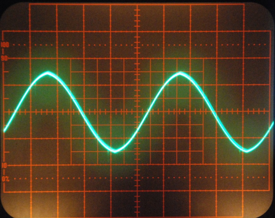
Sine wave audio signal at U1 Pin 6.
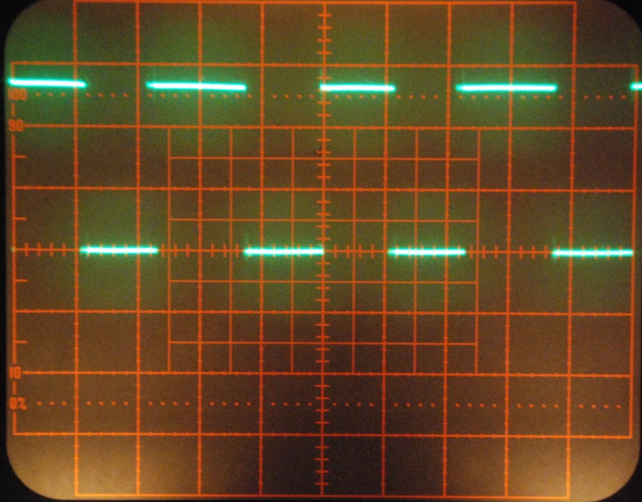
Double frequency square wave at U2D pin 8.
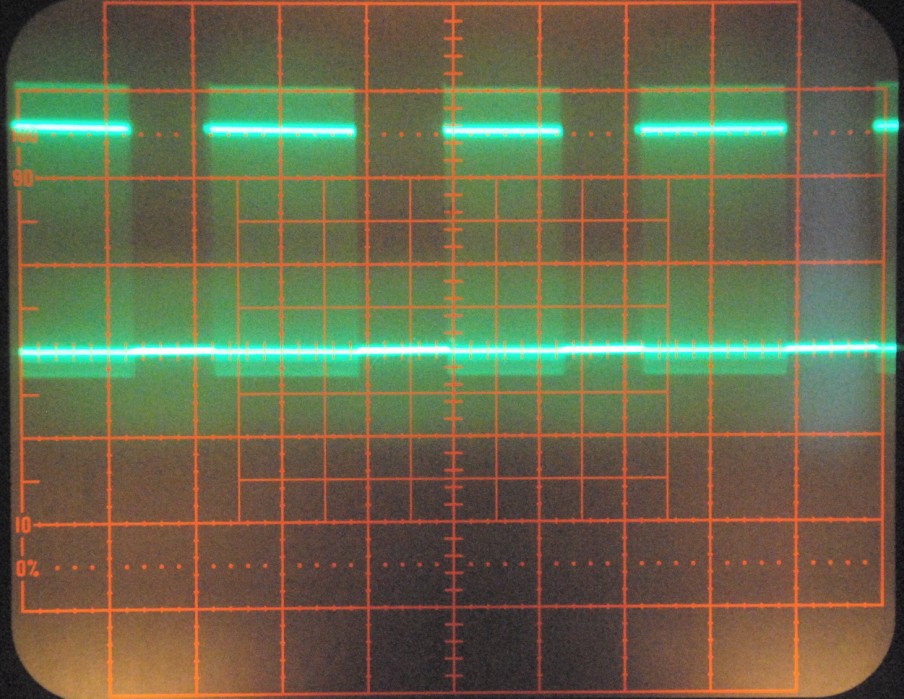
3.1 MHz Oscillator signal at U4 Pin 5.
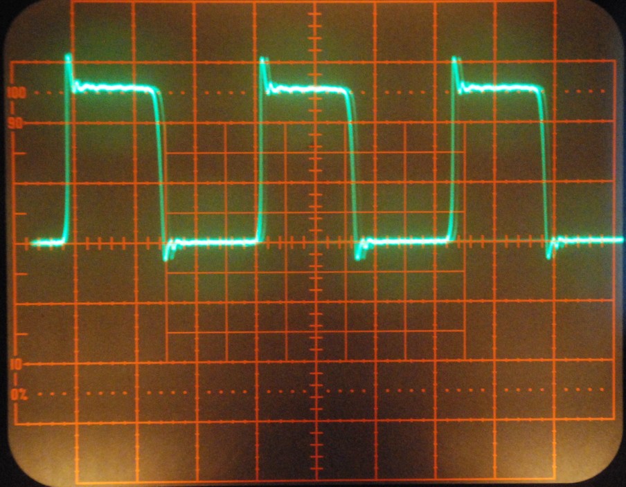
Square wave modulated 3.1 MHz carrier signal output at U3 Pins 5 and 7.
Next, we'll take a look at the actual system as-built and describe the remainder of the hardware.
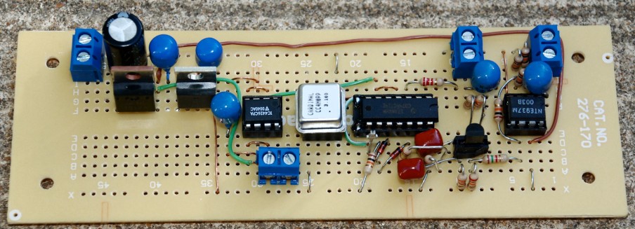
This is the prototype Control Logic board before installation in the case. Resistor R2 had not been added at this point.
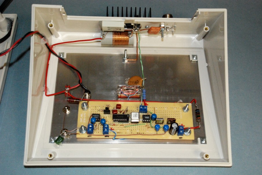
The prototype control board installed in the cabinet. Potentiometer R3 had not been added yet. The balance meter is seen directly above the circuit board next to the blue resistor. The tank coil for the IPA is above the aluminum panel, and below the black heat sink. The twisted pair of thin wires between the IPA and the circuit board caries the RF drive from U3 to the MOSFET in the IPA.
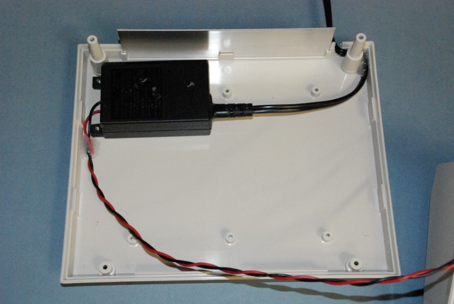
The 28 volt power supply is attached to the inside of the enclosure. The supply was salvaged from a discarded HP inkjet printer.
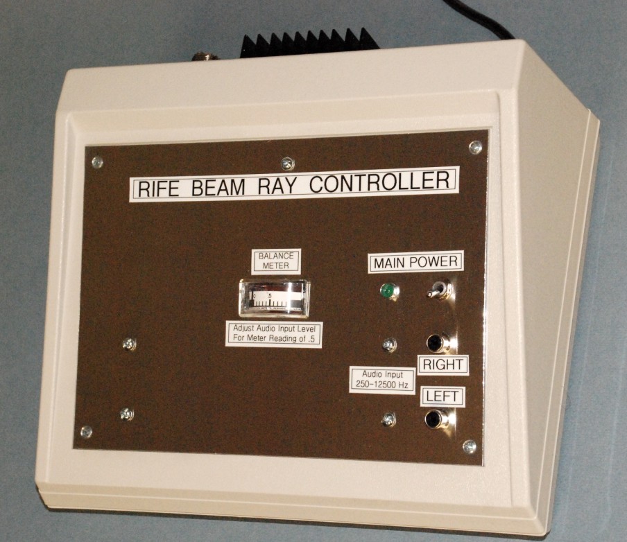
The assembled controller before R3 was added. Note that there are two audio input jacks on the front panel. This is for convenience only, since most CD and DVD players have two audio output connections. The two jacks are connected in parallel inside the enclosure.
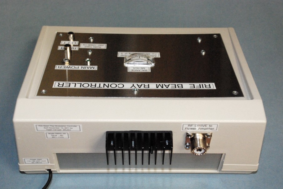
The rear of the controller enclosure showing the RF output connector from the IPA to the final RF power amplifier. The black heat sink is the heat sink for the IRF510 MOSFET in the IPA.

Here is the controller in use. Note that the audio gain potentiometer R3 has been added to the left of the Balance Meter. The Balance Meter reads about mid-scale, which represents a 50% duty cycle output. Note that only one audio input jack is in use. I made an adapter cable between the DVD player and the Controller which connects both audio outputs of the DVD player together.
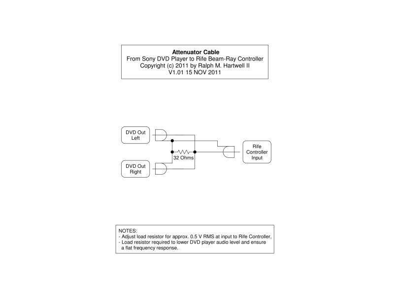
If you are going to use a DVD player for your audio source, you will likely need to attenuate the audio output from the DVD player to avoid overloading the Controller Logic Board input. Standard attenuator cables will likely roll-off the high frequencies excessively. This will show up as the need to constantly readjust the audio level as the frequency sweep progresses. If the frequency response of the system is "flat" (uniform) then you can "Set it and forget it." Please click here for a PDF copy of this diagram.
The circuit shown here for an attenuator cable loads the audio output line(s) of the DVD player with a low impedance load so the response stays flat. It also combines both audio channels into one so you need only one cable going to the audio input of the Controller Logic Board. The value of the 32 Ohm resistor may be adjusted as necessary for your audio source. If you have installed audio gain potentiometer R3, then set R3 to mid-scale and adjust the value of the 32 Ohm resistor for a mid-scale reading on the Balance Meter.
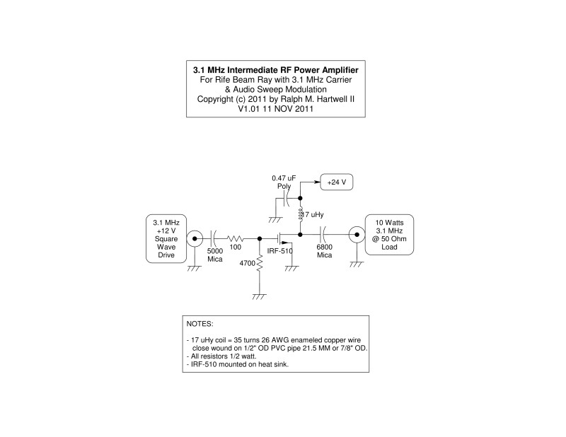
Here is a diagram of the Intermediate Power Amplifier (IPA.) It's pretty straight-forward. It is designed to boost the output of the Control Logic Board up to about 10 watts in order to drive a larger RF power amplifier which will in turn drive the Rife Tube. For a PDF copy of the diagram, please click here.
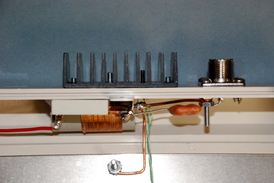
This view of the IPA shows the heat sink attached to the rear of the plastic enclosure. A hole is cut through the plastic enclosure so that the IPA MOSFET may be directly bolted to the heat sink.
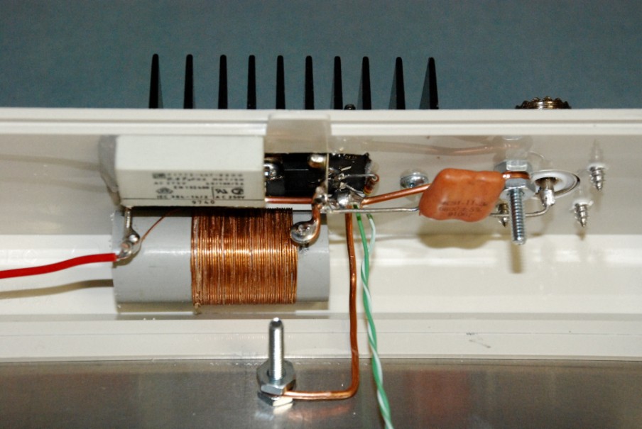
This view from a slight angle, shows the 4700 Ohm bias resistor that is soldered directly across the MOSFET's pins. The RF output connector is seen to the right of the brown 6800 pF mica capacitor.
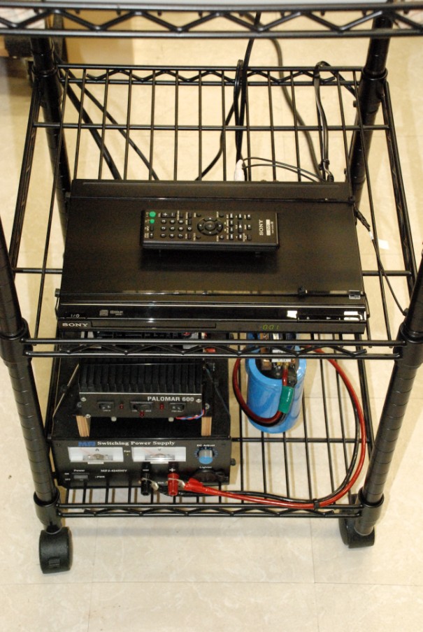
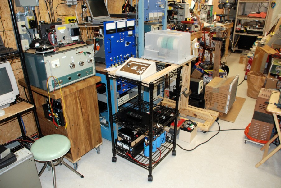
This view shows the DVD player on the middle shelf of the roll-around equipment rack which is used to hold the completed Rife Beam-Ray system. The 12 volt DC power supply is on the bottom shelf. On top of the power supply is the PE-600PL amplifier. The large blue filter capacitors to the right of the power supply are used as surge capacitors to prevent the switching power supply from shutting down on modulation current peaks.
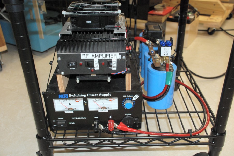
A better view of the amplifier and power supply.
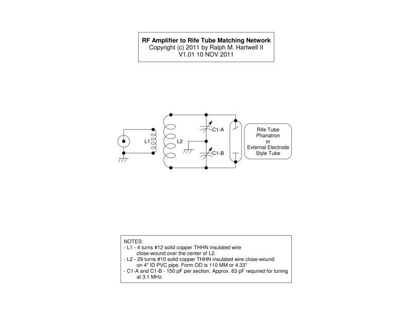
This simple schematic shows how little hardware is required to match the RF amplifier to the Rife tube.
Please click here to download a PDF copy of this file.
The commercial antenna tuner that is usually used to match the RF amplifier to the Rife tube may be replaced by using this circuit.
The difficulty in matching a Rife tube to an amplifier is because when the tube is off between RF pulses, the tube behaves as an open circuit, therefore when the next RF pulse appears, the antenna tuner will see the Rife tube as an in finite impedance, which it cannot match. Conversely, when the tube is lit, it appears as a very low impedance load to the antenna tuner. In order to use an antenna tuner, it is necessary to misadjust the tuner so that it is set at a compromise setting between an infinite and a low impedance. This results in less than perfect power transfer between the RF amplifier and the Rife tube. This mistuning also increases the internal loss in the antenna tuner, wasting valuable RF power.
What is needed is a way to produce a high RF voltage at the start of each RF pulse to light the Rife tube, and then provide a way to couple the RF power into a fairly low impedance load when the tube is lit. Here's how this matching circuit accomplishes this difficult task.
RF power from the 50 Ohm output of the RF power amplifier is applied to the input of the matching circuit and drives the link coil, L1 (the black winding on the coil in the photograph, below.) The link coil couples energy magnetically into the secondary winding, (the Tank coil.) Variable capacitor C1-A and C1-B is used to tune the Tank coil to resonance at the carrier frequency, in this case, 3.1 MHz. The electrodes of the Rife Tube are connected to the ends of the Tank coil. The electrodes may be either internal or external to the Rife tube.
When the Rife tube is not lit, it appears as an open circuit to the Tank circuit. The Rife tube electrodes present a very slight additional capacity across the ends of the Tank coil, but this is accounted for by adjusting the tuning capacitor C1 when the Tank circuit is tuned to resonance.
When RF power is applied, the Tank circuit, being at resonance, will build up a very high RF voltage across the ends of the Tank circuit. This high RF voltage will also appear on the electrodes of the Rife tube, causing the tube to light up.
As soon as the tube lights, its impedance instantly falls to a very low value, which causes the Tank circuit to behave as a highly damped resonant circuit. This causes the voltage across the resonant circuit composed of C1 and L2 to decrease to a lower level. This lower voltage level is determined by the turns ratio between L1 and L1, and the coupling coefficient between them. The result of this change is that the RF amplifier "sees" a more efficient load, and delivers RF power to the Rife tube with low loss. Adjustment of the system is simple. Just adjust the value of C1 for the brightest light in the Rife Tube and it's set to go. Construction is simple - just a length of PVC drain pipe, some electrical house wire, some brass hardware, and a variable capacitor.
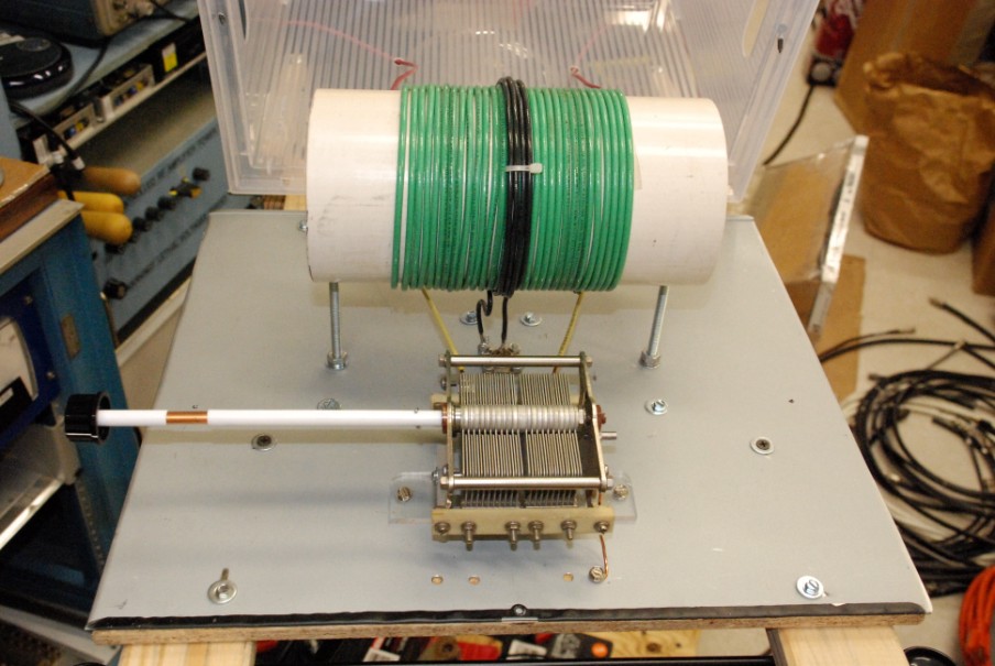
In this prototype circuit, the matching circuit is mounted on a scrap steel plate fashioned from the top cover of a discarded VCR. The plate is screwed to a piece of plywood. The tank and link coil is spaced away from the metal plate by approximately the coil diameter. Note that the steel support hardware is well away from the coil windings to prevent excessive induction losses. The ends of the green Tank coil L2 are connected to the fixed plates of the split-stator tuning capacitor by the two yellow wires. The frame and rotor of the variable capacitor is connected to the metal base plate. The shell of the RF coaxial cable connector is bolted to the metal plate. This prevents RF feedback along the coaxial cable between the Matching circuit and the RF amplifier.
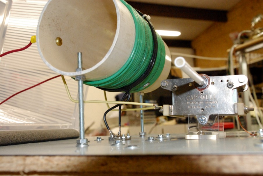
This shows the method of mounting the Tank Coil to the base plate using threaded rod and nuts. The yellow connecting wires between the tuning capacitor and the ends of the Tank coil may be seen passing under the tank coil coil. The black link coil L1 may be seen connecting to the center pin of the coaxial RF connector and also to the metal plate. The capacitor is spaced away from the metal plate by using plastic "L" brackets. Initially, the rotor and frame of the variable capacitor were left ungrounded (floating) but it was found to work better if the frame and rotor was grounded. Metal "L" brackets should be used instead of plastic. The white shaft extension on the tuning capacitor was for insulation when the frame and rotor of the tuning capacitor were ungrounded, but like the brackets, a metal shaft could be used here instead.
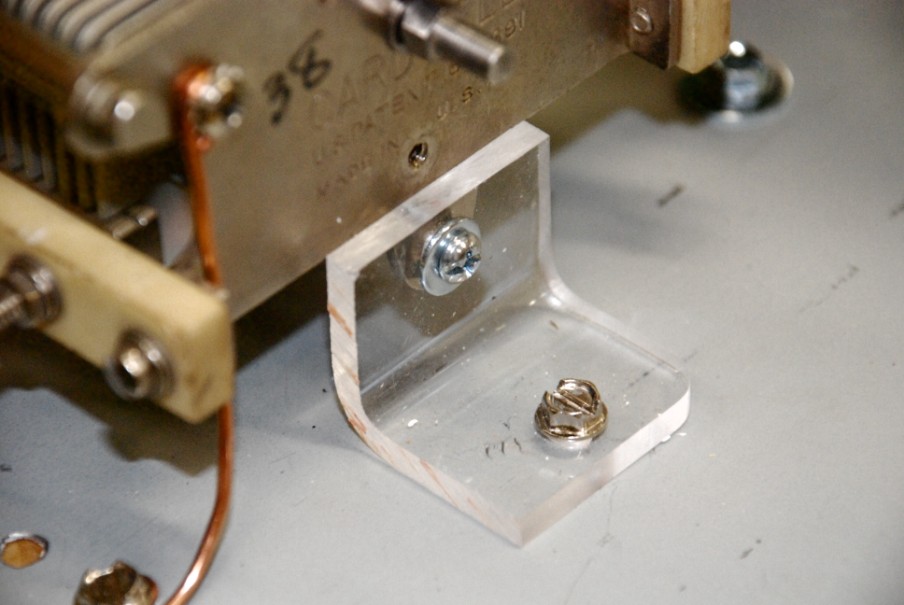
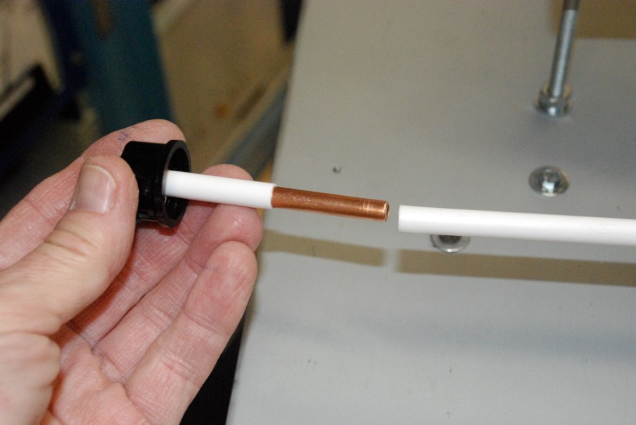
A close up view of the plastic mounting bracket for the Tuning Capacitor C1.
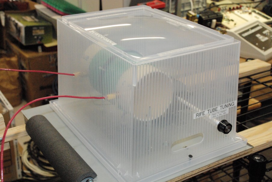
The Matching Coupler is enclosed in an inverted plastic carrying box. The tuning shaft for C1 has been extended through a hole in the side of the box for easy adjustment. The box is held down to the base by using several screws passing through the lip of the box and into the wood base.
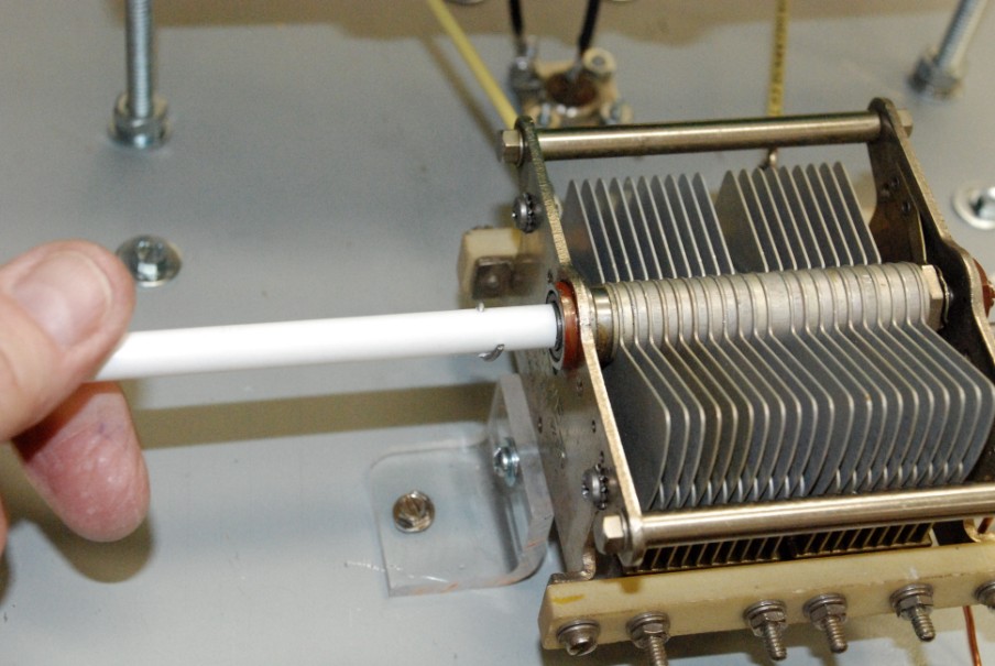
The shaft extension was fabricated from the barrel of a discarded ball point pen. It is a slightly loose fit over the shaft, and so to prevent it from slipping, the capacitor shaft was drilled crosswise and a short length of wire was placed through the hole and through the plastic tube. The ends of the wire were bent over to prevent the wire from falling out of the hole.
Because the plastic tube was too short to pass through the wall of the plastic box, it was necessary to extend the length a few inches. As it turned out, a short length of 1/4" OD copper tube was a very snug fit inside the plastic tube. I used a short length of the copper tube as a splice between the plastic tubes.
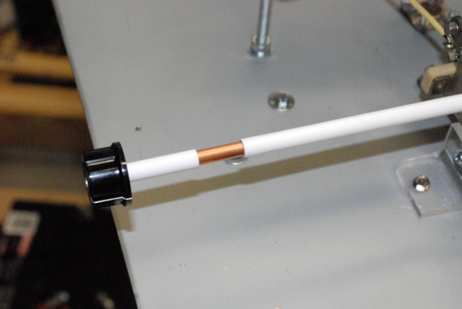
It fit very well.
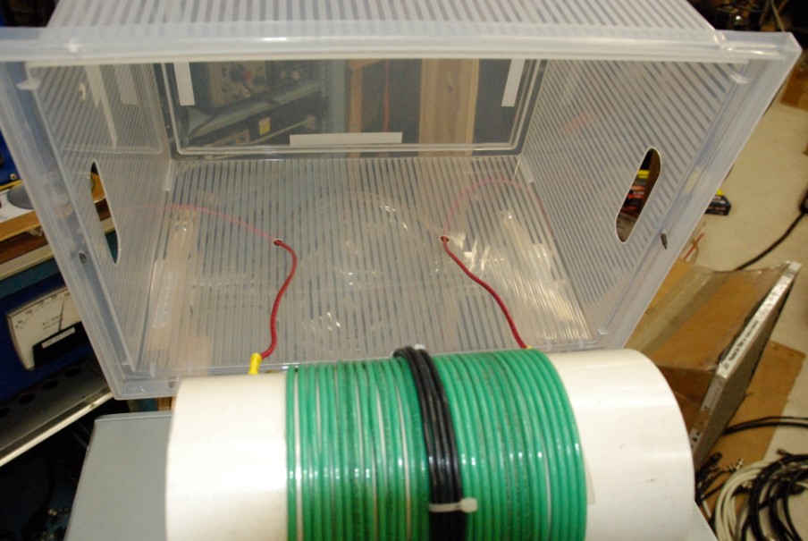
The red wires connect the Tank coil to the Rife Tube. The wires pass through small holes drilled in the front of the plastic box near the coil terminals.
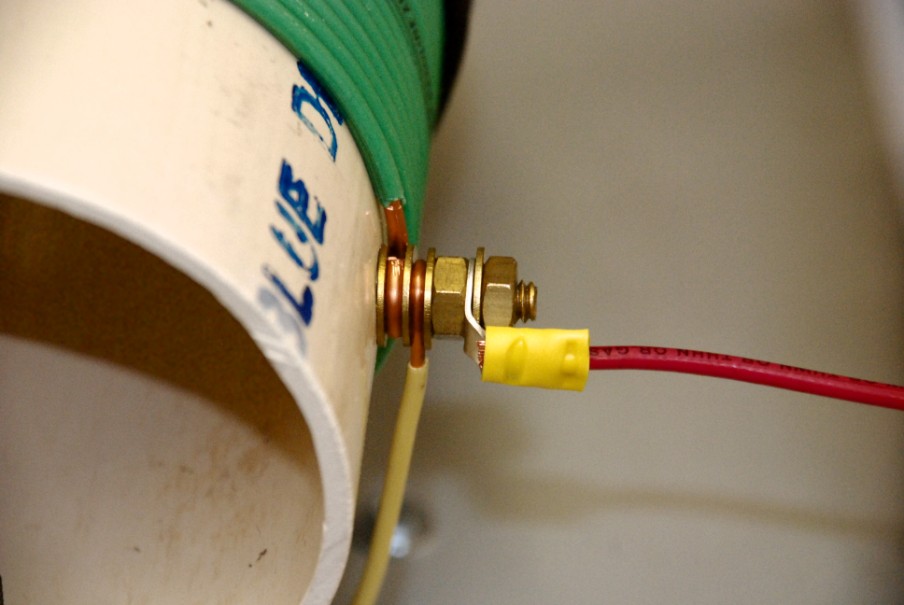
All RF connections to the coil are made with 1/4" brass bolts, washers and nuts for low RF loss. Avoid iron or steel, as it will cause heating!
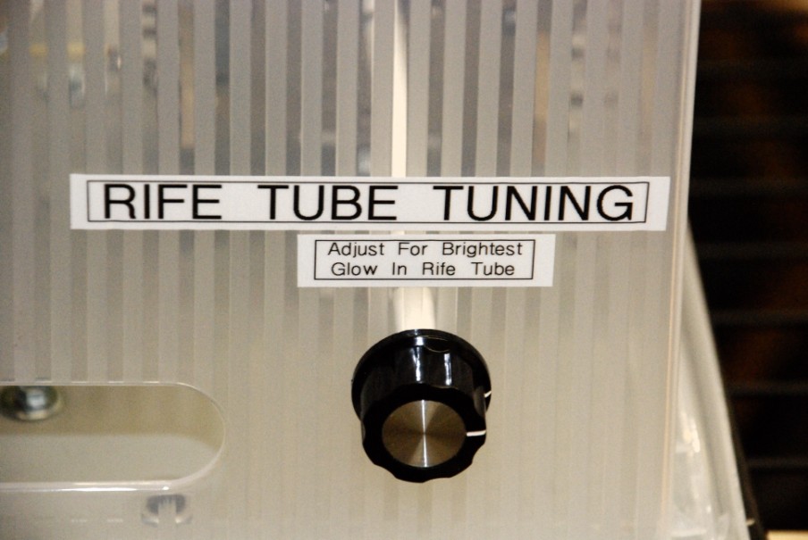
Other than the adjustment for audio level, this is the only control on the entire Rife Beam-Ray system.
Operation is easy: 1) Turn on the power. 2) Adjust the audio level. 3) Turn on the RF power amplifier. 4) Do what it says on the label above the tuning knob. 5) Enjoy!
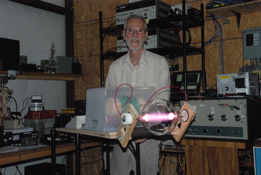
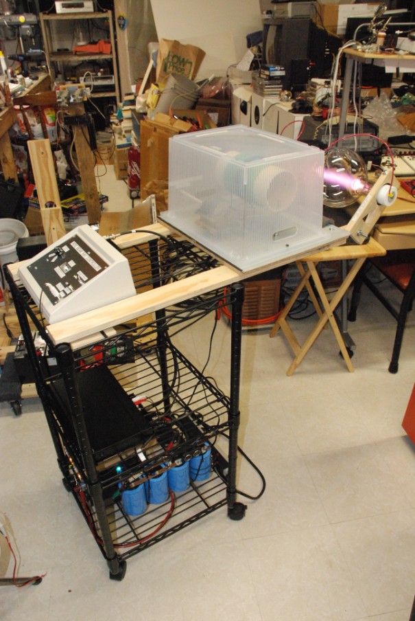
The completed Rife Beam-Ray system prior to undergoing final testing in the author's laboratory.
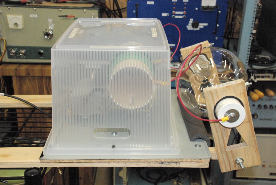
A close-up showing the Coupling network covered by the inverted plastic box.
The Rife tube is supported by a pair of movable wooden arms which hold the tube firmly but gently. The movable arms allow the Rife tube to be positioned over a range of motion to allow placement of the tube next to the item to be exposed to the Rife beam. As shown here, the Rife tube is swung fully back against the foam stop which holds the tube in position for transport or storage.
Note that both the coupler and the Rife tube are cantilevered past the side of the rolling support rack. This allows the unit to be wheeled up close to the experimenter's work while leaving room under the unit for a table or chair, or whatever may be in the way. If you build a system in this manner, please be sure the stand is heavy enough so that the unit does not tip over and smash the Rife tube on the ground!
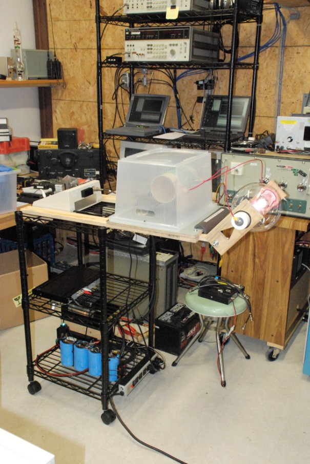
The finished unit undergoing a 4-hour run test.
The Rife tube is positioned 45 degrees out from the storage position. The red wires connecting the Rife tube to the Coupling system tank coil are just long enough to allow the Rife tube to move freely throughout its arc of travel without binding.
Another view of the system undergoing testing. As this is a prototype system, it was not constructed for beauty; just functionality.
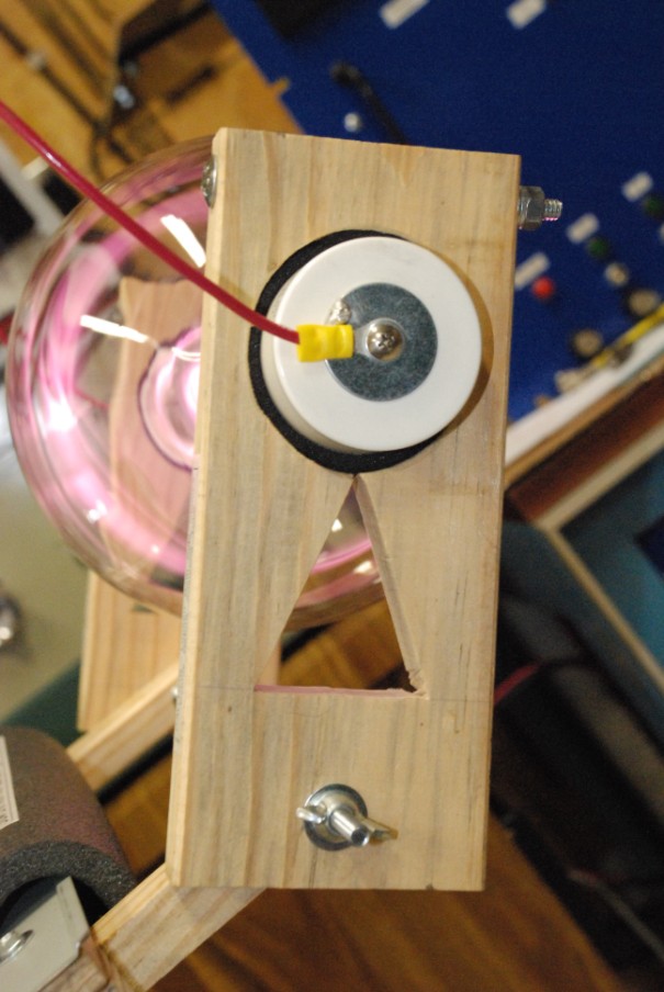
A look at one of the mounting arms for the Rife Tube.
The lower bolts and wing nuts allow for quick and easy adjustment of the Rife tube position. The top through bolts squeeze the wood arm together. There is a narrow slot cut from the top of the open triangle through the hole where the end of the Rife tube fits, all the way to the top end of the support arm. In this picture, the top through bolts have clamped the top of the cut together, "putting the squeeze" on the black foam rubber which wraps around the white plastic end cap of the Rife tube. The triangle shaped cutout in the support arm allows the wood to flex sufficiently to allow the top through bolts to clamp the tube. Without the triangular opening, the wood was too stiff to clamp shut.
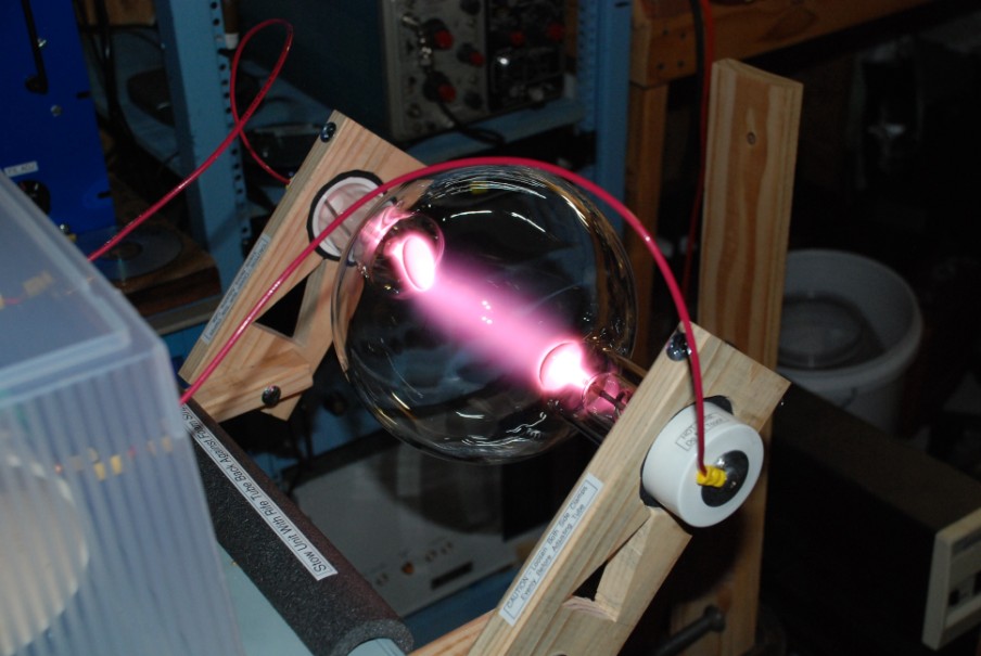
The Rife tube produces a nice glow discharge when it is in operation.
This is very close to how it appears to the naked eye when the tube is powered with 300 Watts peak RF power at 3.1 MHz modulated by a 50% duty cycle square wave.
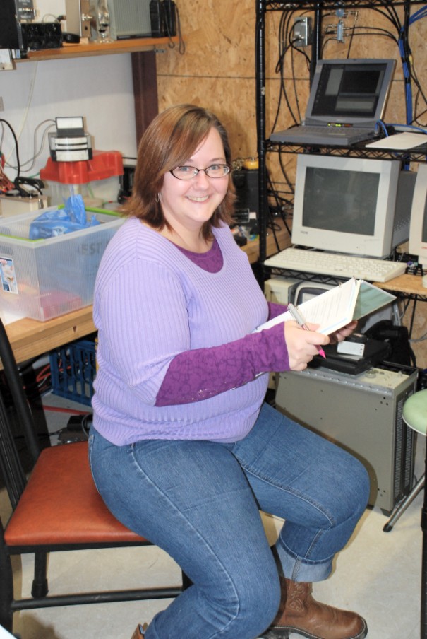
Here's my editor-in chief, Cat, KC5CAH proof-reading the second draft of my instruction manual for the system. She always has her purple pen at the ready!
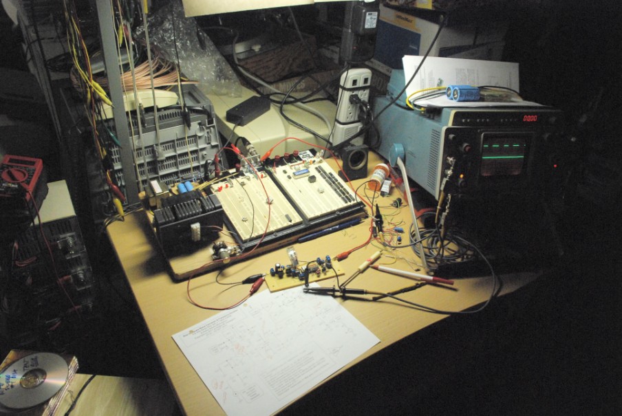
And last, but not least, this is the prototype bench where I let the smoke out of components while designing a new circuit.
On the bench is the prototype Rife Beam Ray Controller Board #1 undergoing smoke testing. (It passed.) The square wave modulated 3.1 MHz carrier signal is visible on the screen of the oscilloscope.
- 73 -
[ Home ]
This page and all text, data and photographs are Copyright © 2011 by Ralph M. Hartwell II, All Rights Reserved.