Experimental KW Switching Power Supply
Initial Design and Test Report - UPDATE #1 (March 21, 2004)
By W5JGV
Click HERE for a PDF copy of a hand-drawn schematic of the test setup.
This is an update of the ongoing narrative of my attempt to construct a high-power switching power supply to replace the failed power supply in my Heath Warrior amplifier. Since I use the amplifier for experimental (non-Ham) work, it sometimes has to operate at full CW power for several hours at a time. The original plate transformer is unsuitable for that task, so I am attempting to build a really heavy-duty supply to replace the original power supply.
My first cut at this project was to attempt to use a string of reverse-connected computer switching power supply power transformers in an attempt to get enough power from the system. I also originally wanted to use as many components salvaged from the computer power supplies as I could. This proved to be somewhat impractical, since the power I wanted to obtain turned out to be just over the edge of what I could comfortable achieve and still keep the smoke inside the components.
If you have read my initial episode in this project, you have a pretty good idea of what I did and how things were connected, so I won't repeat everything in detail in this update. I'll just mention what has been changed and why and what the results turned out to be.
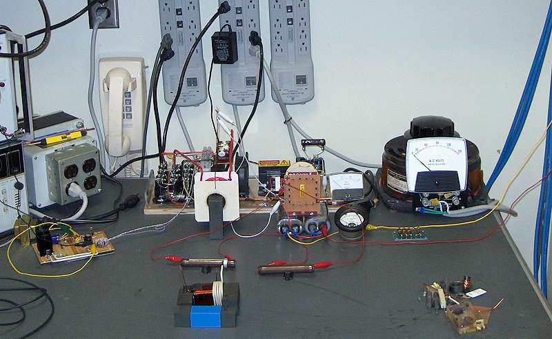
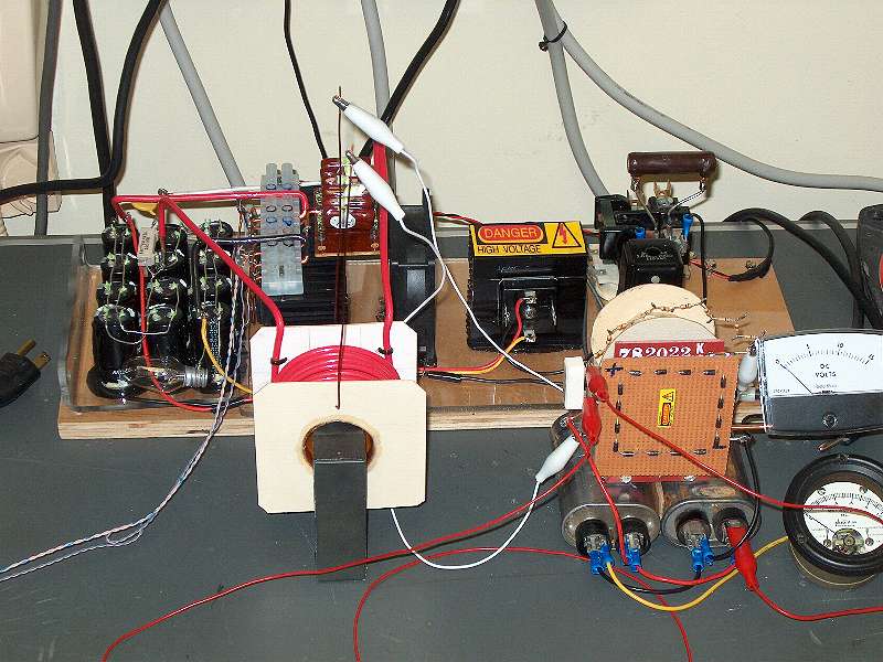
An overview of the test bench setup, affectionately referred to as "Smoke Alley."
From left to right: 2.5 KVA isolation transformer (which keeps the smoke inside the operator); below the isolation transformer is the Low Voltage Power Supply and Switcher Control Board; in the middle visible below the power strips hanging on the wall is the main switching assembly with the new switching transformer and high voltage filter choke and rectifier board. These are sitting on top of two oil-filled capacitors. The high voltage voltmeter and ammeters are to the left of the Variac (which keeps the smoke inside the components); the middle of picture shows two 1,000 Ohm 50 watt resistors which are temporarily used as damper resistors across the high voltage filter choke; in the lower middle is a test switching transformer which is wound on the same size core as the main switching transformer, and in the far lower right is a pile of junk parts I forgot to pick up before I took the picture.
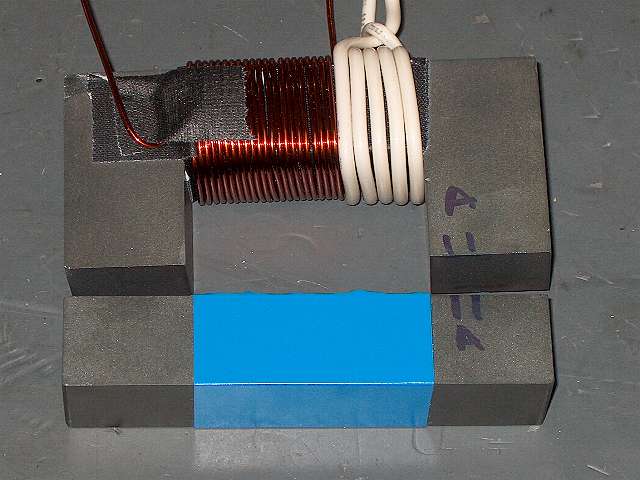
High-power testing indicated that the previous two-section core I assembled from TV flyback transformers was just a little too small to be able to handle a full KW safely. I obtained several much larger cores which should work fine. These measure one square inch in cross section and have a 2" x 3" winding area. The mating surfaces are polished, and they have very low flux leakage. They appear to be made with #77 Material, and allow the transformer to operate with a turns ratio of 10 volts per turn at 40 KHz. I "backed off" from that value just a bit, and am using 7.5 volts per turn in the test transformer.
This particular transformer is one I wound for preliminary testing. I showed it here so that you could see the size of the core. The enameled wire on the core is # 16 AWG, and the white wire is # 12 THHN. The blue tape is for insulation for a test winding (now removed). I had previously scramble-wound about a hundred turns of # 26 AWG wire on the ferrite bar. At 10 volts per turn, that produced a kilovolt when I turned it on!
![]()
This is the finished (well, almost finished) switching power transformer. The coil form is a plastic pill bottle which just happened to fit the ferrite "I" bar quite snugly. The end plates are made from art board cardboard, about 1/16" thick. These are hand-fitted to the plastic tube and then super glued to the tube. Next, the form was thoroughly coated with two layers of my all-purpose plastic coating, clear PVC pipe cement. It was then allowed to dry overnight.
After drying, the secondary winding was wound on the form. It consists of 154 turns of # 18 AWG wire. The wire is larger than actually required, even after factoring in skin effect and current crowding at 40 KHz, but I had a lot of it available, and there was plenty of room on the core for it, so I used it.
To minimize winding self-capacity, after completing each winding layer I applied two layers of fiberglass tape over the winding. I then continued the winding by folding the wire back across the winding so that the next layer started from the same side of the form as the previous winding. This required extra insulation between the folded over wire and the windings to prevent insulation failure.
The primary winding in the finished transformer will be 15 turns of # 10 THHN covered wire. For my initial high power tests, I put 20 turns on the winding. I will remove the extra 5 turns after the preliminary testing is complete. The extra 5 turns on the primary winding limits the output of the system to about 1,100 Volts maximum. Removing the extra 5 turns should boost the output voltage to 1,400 Volts @ 800 MA. I will be able to voltage regulate by using pulse width modulation to reduce the voltage to about 1,300 for the the 811's in the amplifier.
Running this transformer at about 800 watts causes virtually no core heating. It should be possible to obtain about 2.5 KW from this core. The primary winding gets slightly warm at the 800 watt level due to skin effect and current crowding. The use of Litz wire for the primary winding would be a better choice than using solid wire. Another option would be to use a twisted bundle of 6 strands of # 23 AWG insulated wires as an approximate substitute for Litz wire.
After completing the windings, the facing surfaces of the core sections were carefully cleaned and placed against each other, then bound together with Gaffer's Tape.
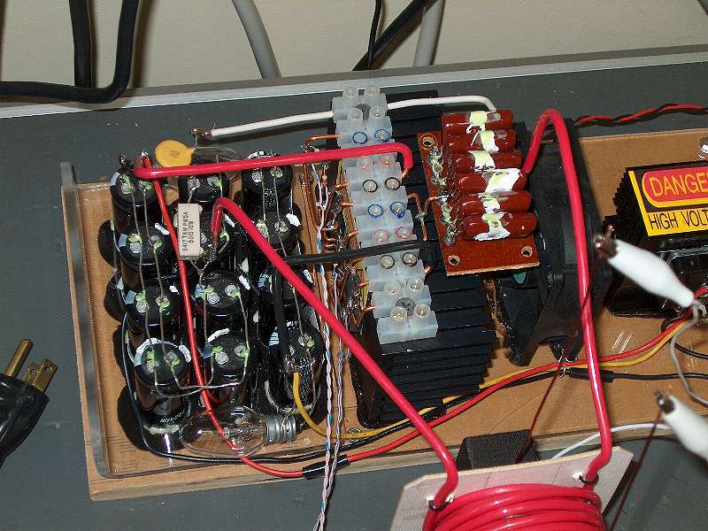
The primary winding of the switching transformer connects to the switcher output capacitor bank (seen here splashed with green and white paint). The other side of the capacitors (which are all in parallel and act as a single 12 uF, 400 Volt capacitor) is connected to the common point of the half-bridge transistor stack (2 transistors) which are mounted on the black heat sink under the white terminal strip. The purpose of these capacitors is to keep any direct current from flowing through the primary of the transformer in the event of an unbalanced switching waveform. Direct current through the transformer windings could cause core saturation and destruction of the power switching transistors.
The + and - 150 Volt filter capacitor assembly has been moved as close to the transistors as possible to minimize the impedance of the wiring in an attempt to eliminate switching waveform ringing and distortion. (It worked, BTW.)
A primary winding damper (snubber circuit) to counteract the effect of the leakage reactance between the primary and secondary windings is the white 50 Ohm resistor and the yellow .0022 disk capacitor visible to the upper left of the picture. These parts are connected in series and are placed directly across the primary winding of the transformer.
Theoretically, it would have been better to have wound the transformer with split primary and secondary windings, because this would have reduced the leakage inductance between the windings. This was not done because tests indicated that for this particular system, a very small reduction in transformer losses would be obtained with split windings, but the difficulty of construction would be more than doubled. In addition, it would have been almost impossible to make any changes to the windings once the transformer was wound with split windings. It was estimated that using the simple method of winding one winding over the other would result in only about 4 watts additional power loss in the snubber network.
The white clip leads connect the high voltage secondary of the switching transformer to the high voltage bridge rectifier and filter assembly which is shown to the left of the meters.
The HV rectifier is a full wave bridge made from 16 type UF4007 high-speed rectifiers. These are matched diodes, and there is no bypassing or equalization placed across any of the diodes. The diodes are mounted on the phenolic perf board which is visible just above the two HV filter caps which were salvaged from a couple of old microwave ovens. The capacitors total 2.2 uF. At 40 KC, this small amount of filtering is very adequate.
The HV filter choke is wound on the salvaged core from a TV flyback transformer. Some experimentation was required to get the right inductance and current carrying capacity without saturating the core. The number of turns and the air gap was adjusted for optimum results.
Visible just to the left of the perf board is a rectangular white power resistor. This is used as an oscillation damper load for the filter choke, which "rings" when the diodes stop conducting. The original value was 1,820 Ohms @ 5 watts. This worked perfectly well when the switched driving waveform was a 50/50 square wave, however when pulse width modulation was attempted at a 20/80 ratio, the resistor erupted in flames within 5 seconds of power on! Measurements showed that it was necessary to increase the power rating of the resistor to 100 watts.
Unfortunately, a considerable amount of power is wasted in this resistor and cannot be recovered. It will be necessary to revise the design of the filter choke to handle the increased harmonic energy generated at short switching duty cycles.
The voltmeter (whose scale reads 0-15 Volts DC), has a string of dropping resistors to scale the meter to read 0-1,500 Volts. The 0-1 MA meter has been shunted to read 0-1 Ampere. These monitor the HV DC output from the power supply.
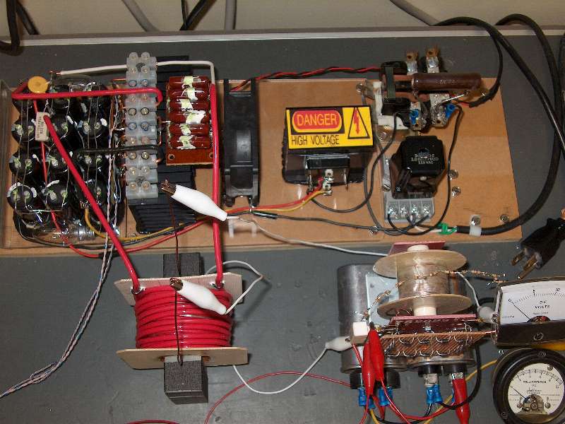
Another view showing the filter assembly and the voltmeter dropping resistor string.
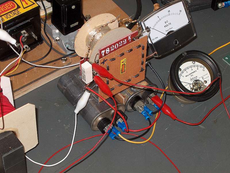
A close up picture of the rectifier - filter assembly and metering. Note the red clip leads connected to the white shunt resistor (now burnt out) they connect to the temporary resistors visible in earlier photos.
Remember - this is a test bench stuff, and will be repackaged for placement in the amplifier; in the meantime, keep your fingers out of the HV!!
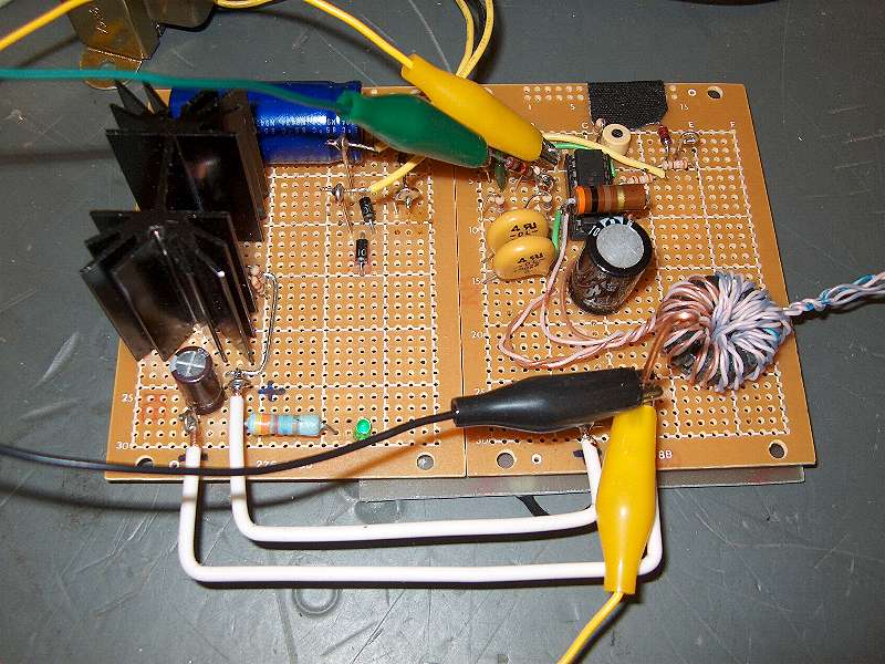
And the last picture - the low voltage power supply and the switching control board.
I changed the power supply from a full wave bridge rectifier circuit to a full wave rectifier and dropped the regulated voltage from 17 Volts to 10.5 Volts because that's all the control chip needed to provide enough drive to the switcher transistors.
I was not able to get enough base drive using the original bipolar transistors, so I switched to a pair of International Rectifier IRG4PC40U IGBT transistors salvaged from another computer power supply. These interesting devices have the gate drive requirements and advantages of MOSFET's, and the voltage and current ratings of a bipolar device.
The switcher control chip (TL494) drives the small toroidal gate driver transformer seen here. The primary is a bifilar winding of 10 turns (10-0-10) and the secondary is two twisted wires of 15 turns each, each of the two wires forms a separate secondary which drives one of the two switching transistors. The gates of the transistors "look" like a 0.0033 uF capacitor to the transformer, so it was necessary to insert a 22 Ohm resistor in series with the gate drive signal to eliminate transformer ringing. The resistor is inserted in the circuit at the gate lead of the transistor. The gate drive signals are fed to the gates via a twisted pair of #26 wire stripped from some CAT-5E cable. - In fact, that's what the little toroid transformer is wound with.
The switching control chip works well, and by using pulse width modulation, it allows me to adjust the voltage anywhere between 250 Volts and 1,100 Volts with the twist of a knob. The finished unit will be provided with both voltage adjustment and automatic voltage regulation to compensate for load changes. Getting that to work correctly is the next part of this project.
I'll post more info in another update when I make further progress.
73,
Ralph W5JGV