
A 400 Watt 60 Hertz Power Inverter
by W5JGV
August 15, 2005 (revised August 18, 2005, July 19, 2006)
What To Do With Those Old Buzz-Box (Vibrator) Inverters.
Over the years I have found that having a 12 Volt DC to 120 Volt 60 Hz inverter is quite useful. I occasionally make repairs to equipment in areas where there is no available AC power to run my power tools. Having an inverter that I can connect to the car battery is a real lifesaver. Yes, I know that there are lots of battery operated power tools out there, and as a gadget freak, I certainly own my share of them. Sometimes, however, it's just easier to be able to run a more powerful tool, soldering iron, electric drill, or whatever, and a good inverter fills the need. The problem is that some of the more modern power inverters are not capable of running a serious power tool.
Digging under the tables at Hamfests will often reveal discarded or deceased square wave vibrator inverters, or early model transistorized inverters, such as the one I show in this article. These units are excellent candidates for conversion to transistorized operation. What I will show in this article is a way to convert one of these older units to fairly stable 60 Hz (60 Cycle to you old guys, like me!) transistorized inverter with overload characteristics similar to the old vibrator driven inverters. This particular unit shown in this article is essentially a vibrator inverter which has been converted to transistor operation. You can convert any inverter of this type or a vibrator inverter according to this article and it should work just fine. Note that the newer "build a waveform" inverters use very small transformers and are not suitable for this method of conversion - they don't operate on the same principle.
The use of transistors in power inverters has greatly changed the internal design of power inverters. The first inverters available in the 1940's used a vibrator to drive a transformer to convert 6 or 12 Volts DC to 110 Volts AC. The vibrators used in these power inverters are the big brothers of the smaller 4, 5 and 6 pin plug-in metal can vibrators used in car radios of the 1940's and 1950's. These power vibrators came in larger sizes and could handle substantially more power then their smaller kin.
The internal design of the vibrator inverter is fairly simple. DC comes into the unit, and is chopped into square wave pulses by the alternating contacts of the vibrator, which acts as a single pole double throw switch. These pulses are then fed first to one end of the center tapped primary winding of the inverter transformer, and then to the other end of the primary winding. This alternating series of DC pulses simulates an AC square wave which the transformer steps up to 120 volts AC on the secondary side. The power limit on this type of inverter is usually how much current the inverter contacts can handle before they melt. (That happens more than you would expect.)
In normal operation, the oxide film on the Tungsten vibrator contact surfaces and the bulk resistance of the contacts causes a small voltage drop across the contact points when they are closed and carrying current. This drop is in the order of 0.05 to 0.20 volts, depending on the current and condition of the contacts. Since the vibrator assembly is built into a closed and soundproof case (there's a reason we called 'em Buzz Boxes!) to prevent contaminants from entering the vibrator case and damaging the contacts, it's hard for heat generated by the contacts and the vibrator coils to escape. Because of this, the vibrator is usually rated at somewhat less current that the contacts can ultimately handle. However, the vibrator can intermittently handle some current above it's normal rating if the operator is careful. Fuses are absolutely essential with a vibrator inverter, because since the vibrator is just an oscillating switch, it will try to pass whatever current the load is demanding. That's why the vibrator inverter is so nice; you can run anything on it as long as you don't cause a meltdown.
Present day power inverters are much smaller in physical size, and they can handle a lot more power than the older vibrator driven units. However, I have found that many of the new inverters are unable to handle much of any overload without "dumping" and shutting off. For example, trying to run a 14" color set on a 300 watt rated inverter resulted in the inverter shutting down on overload. The TV set is rated at 120 watts, and the inverter is rated at 300, so what's the problem? Well, when the TV set is turned on, it draws a big surge of current to charge the filter capacitors and operate the degaussing coil surrounding the picture tube. This surge shuts down the inverter. An old style vibrator driven inverter will just grunt a bit and then carry on, starting the TV and running it in fine fashion.
I have a large Radiart vibrator that is in a case that measures about 5" x 3" x 3" in size. It has two 6-prong plugs on it to handle the power. It is driven by two electromagnets and requires about 25 watts at 12 Volts DC just to run it. It has a total of 16 switching contacts, not counting the contacts used to drive the vibrator coils. It's a real beast of a vibrator, but it can handle the power! I use it in the original inverter, which was rated to handle 300 watts - at 6 volts! That's a current drain through the contacts of about 50 amps! Not bad for a buzzing relay.
I discovered that the transformer was actually made with 4 -6 volt windings in parallel, so I was able to reconnect the transformer to make it work on 12 volts. I found that the transformer had enough iron in it to handle more power, and I found that I could now get up to 600 watts out of the unit. Remember what I said about meltdown? Well, I found that with that big vibrator, I could actually run my 6" circular saw from the inverter. Not for too long, though, but it is still impressive. None of my newer transistorized units will do that.
Still, one day, the vibrator will expire, and then I'll have to figure out something to replace it with or scrap the unit. This particular vibrator is no longer available. It cost me better than $50.00 USD back in the early 1950's; I hate to think of what it would cost today, if it were still available. The logical option (these days, anyway) is to think "Solid State!"
Modern inverters use a bunch of transistors to replace the vibrator. There are three types of units commonly available. One type "builds" a sine wave out of high frequency pulses which are summed into a sine wave by a transformer / low pass filter system. These are used for loads that require actual sine wave power. Most equipment is not so critical as to their power requirements, and they may be operated on what is termed a "Modified Sine Wave" power source. This is usually a square wave AC waveform, with a long dead time between the positive and negative portions of the waveform. The result of this waveform is to greatly reduce the harmonic content of the waveform as compared to a simple square wave. The third (and earliest) inverter simply generates a square wave output. Most, but not all, devices will operate satisfactorily on a square wave. In addition, square wave inverters are simple to build when compared to sine wave or modified sine wave inverters.
The conversion described here will result in a square wave output, which is what these older vibrator / transistorized inverters produced originally. I've converted four of these units so far, with excellent results in each case. One advantage of converting these units is that they are much more electrically quiet than the vibrator units. The contacts in a vibrator inverter always exhibit some amount of sparking and that sparking causes RFI. Noise suppression is accomplished in these units by using carefully chosen high voltage buffer capacitors placed across the transformer windings and sometimes across the vibrator contacts as well. Failure of a buffer capacitor - they always fail shorted - often results in a set of melted vibrator contacts. After conversion as shown in this article, RFI is a thing of the past, unless you do a poor job of construction. In that case, it is possible for the MOSFET's to oscillate at VHF and cause interference. That problem is easily solved by placing a very small ferrite bead over the gate leg of the MOSFET's.
This was a nice on-the-table Hamfest find - a 400 watt combination inverter / battery charger. The fellow who sold it said he could not find replacement transistors for it, so he was selling it to clean out the shack. As it was originally designed, it used a total of 10 PNP TO-3 power transistors to handle the 12 Volt DC power and generate a clean square wave output at 117 volts 60 Hz. The transistors were toast, and a replacement set would cost over $100.00 USD, so something else was definitely in order! The transistors were also used as the battery charger rectifiers, but since the voltage regulator circuit was missing when I obtained the unit for $5.00 USD, I decided to strip the unit and start over. This picture shows the unit after conversion. I did not bother to paint it or dress it up, as it will be a "workhorse" unit used in the field.
What I decided to do was to replace all of the PNP transistors with some high power MOSFET transistors which have very low voltage drop when they are turned on. In that respect, they behave much like a vibrator. By using high current rated transistors, excellent overload capacity is available. The required square wave gate drive for the MOSFET's and the 60 Hz frequency control is provided by a low power cross-coupled oscillator using a small filament transformer that is driven into core saturation.

This view of the modified inverter shows a 1/4" diameter bolt and washer near the rear (left) of the cabinet. The bolt holds an aluminum block against the chassis for cooling. A pair of MOSFET's are mounter on the thermal block. Note the white plastic electrical insulation between the washer and the chassis. The bolt is electrically "hot" because it is connected directly to the cases (drain connection) of the MOSFET'S.

Here's a top view of the modified inverter. In the center is the output transformer. Since it if used at 60 Hz, it is big and has lots of iron in the core. Newer high frequency inverters will have very small ferrite core transformers in them. Note the heavy gauge wire of the primary winding, which is wound over the high voltage secondary winding. The four power MOSFET's I used in this conversion are mounted in pairs on the rectangular aluminum heat spreader blocks which are visible to the left and right of the case. The primary winding snubber RC network is visible as the "EVOX-MMK" capacitor and the two blue resistors to the right of the capacitor. The small transformer mounted on the left side of the chassis is the oscillator transformer. The snubber network are required to handle the energy stored in the leakage reactance of the output transformer. If the snubbers did not eliminate this energy, potentially destructive high voltage spikes can occur during the switch time and destroy the MOSFET's.

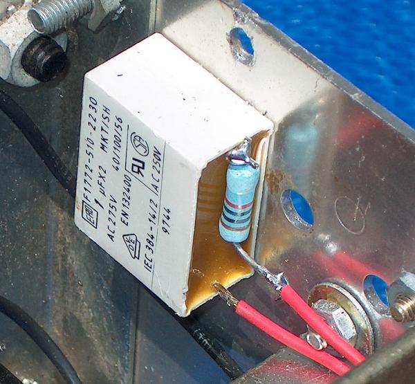
Bottom view of the modified inverter. The blue capacitor with the white paint on it is connected across the secondary winding to clean up the waveform. It reduces the high frequency secondary ringing to a lower frequency and reduces the amplitude of the ringing. I used the ammeter which was part of the original unit (the meter is visible in the lower center of the photo) as it is handy to be able to check the load current drawn by the inverter. The two original POST style 3AG fuse holders were left in place and used in this conversion. They each contain a 20 A fuse. They are placed in parallel. If I were to build a new unit, I would have used the newer and less expensive automotive fuseholders and fuses.

This is the oscillator. The filament transformer is driven to saturation at a 60 Hz rate by the pair of NPN transistors mounted just above the heat spreader block for the MOSFET's The red and blue resistors set the base drive for the oscillator transistors and adjust the frequency of the oscillator.

Keeping the oscillator DC supply voltage steady is necessary in order to maintain the frequency at exactly 60 Hz. A 50 watt Zener diode is used to regulate the supply voltage. Zener diodes can hold voltages more accurately than most 3 terminal voltage regulators. Since this Zener diode was already in the unit when I obtained it, I decided to make use of it. The large rectangular white resistor (salvaged from an old TV receiver) provides current limiting for the Zener diode. With the component values shown on the diagram, the gate drive and the output frequency is constant at all DC input voltages from 8.5 to 16.5 Volts. The Zener diode is mounted on the other side of the chassis where the red and yellow wires are soldered to the diode pins.

The case of the Zener diode is grounded to the case, but I used some heat sink compound between the case and the chassis to ensure good thermal contact. Because the oscillator frequency is determined by both the DC supply voltage and the base drive of the oscillator transistors, the Zener diode was used to hold the oscillator supply voltage constant. (More about this in the schematic discussion.)

Here's a close up of the oscillator transistors and the one of the MOSFET pairs. I can't say much for the neatness of the solder joints, but they are secure. I think I soldered, unsoldered, and resoldered a zillion resistors until I found the ones I needed to get the correct frequency. Note to self: Next time, use a potentiometer!!! The transistors are insulated from the chassis with some thermally conductive insulators I salvaged from some old computer power supplies. The transistors also came from computer power supplies. In fact, so did the nuts and bolts I used to mount the transistors to the chassis. Computer power supplies and computer monitors are a treasure trove of small parts for homebrewing electronic equipment!

Although the diagram shows a pair of MOSFET's in the output circuit, there are actually four transistors used. Each end of the output transformer is driven by a paralleled pair of MOSFET's. Note that they are mounted as a parallel pair on an aluminum block. The Drain (case) of each transistor is bolted directly to the block with no insulators. This is to maintain the temperature of each transistor in the pair as identical as possible. Maintaining identical device temperatures allows the transistors to more closely track each other electrically when in operation. The aluminum block is electrically insulated from the chassis by a section of plastic sheet insulator that was salvaged from a computer power supply. I tested it for good heat transmission, and it was adequate for this job.
Each of the MOSFET's used here can handle at least 65 A, so a single pair should be sufficient to do the job in this inverter. Why did I "double up" on the transistors? The voltage drop across a MOSFET (the conduction loss) when it is switched on increases in proportion to the current passing through the MOSFET. Placing two MOSFET in parallel, causes each one to carry just half of the total current. The forward current voltage drop in a conducting MOSFET has a positive coefficient of temperature. This means that as the MOSFET gets hotter with increasing current, the internal resistance of the MOSFET will increase, which then increases the voltage drop across the MOSFET.
Placing two MOSFET's in parallel causes each one to carry half of the total load current. Whichever MOSFET happens to conduct slightly better than the other one (transistors are never exactly identical) will get a little hotter, which will increase it's resistance, and the resulting increase in voltage drop across the MOSFET will cause the other MOSFET in parallel with it to conduct more of the total current. This effect automatically forces the MOSFET's to share current evenly when they are operated in parallel.
Even better, paralleling MOSFETS results in something for nothing - the total power lost in heat is half of the loss when just one MOSFET is used. For example, assume that a single MOSFET drops 2 volts when carrying a current of 2 amperes. The loss is then 2v X 2a = 4 Watts. Splitting the current between two MOSFET's results in 1 ampere of current through each MOSFET, but since the voltage drop is proportional to the current, the voltage across the MOSFET's falls to 1 volt. Now the power loss for each MOSFET is 1v X 1a = 1 Watt times 2 transistors = 2 watts total loss. Not only have we decreased the total heat loss in the circuit by half, we have reduced the heat loss in each MOSFET to one-fourth of the original value.
At high power, this can mean the difference between comfortable operation and blown transistors. Using the aluminum heat spreader block allows sudden heat surges generated under overload conditions to be rapidly removed from the transistors and dissipated over a larger chassis area than would be possible if the transistors were bolted directly to the chassis without the use of the Aluminum block.
It is important that the MOSFET's are mounted so that their leads can be connected together with short leads. This is necessary for proper current sharing and to prevent VHF oscillations. The heavy copper wire from the MOSFET source leads to the chassis may be seen in this picture.
MOSFET's are good choices for power inverter use, because the I^R power loss and the resulting heat generated at full power operation are less than the losses in bipolar devices. The combination of the thin (1/8") aluminum chassis and the aluminum block provides sufficient heat sinking for the MOSFET's. The thermal mass of the heat spreader blocks and the surrounding chassis material allows overload operation up to 700 watts for several minutes. (The fuses blow out at that point.)
This is the RC snubber network that is placed across the winding of the oscillator transformer. It is used to clean up the waveform and helps produce a clean square wave from the oscillator. Note that all three capacitors used in this modification have been salvaged from used computer power supplies. The capacitor is attached to the chassis the lazy Ham's way - I Super Glued it there!!

A close up of the RC snubber that is placed across the primary of the output transformer. This network takes care of the energy stored in the leakage inductance in the transformer. The network is "tuned" by adjusting the R8 and C2 values for the minimum waveform "ringing" (transient oscillations") as seen on the drain of the MOSFET's. This adjustment needs to be balanced against the minimum crossover (switching) waveform spike as seen at no load. Allowing the switching spike to get too large can result in failure of the MOSFET's. Note that changing the value of C3 will require adjusting the values of the R8 and C2, seen here.

This is waveform correction capacitor C3. It must be rated for at least 250 volts AC. This capacitor was salvaged from a computer power supply.
If you've followed me this far, it's time to take a look at the schematic diagram and the specifications for some of the components. These are all PDF files.
Schematic diagram of the inverter
Data sheet for the 1N2805 Zener Diode
Data sheet for the 2SC2625 transistor
Data sheet for the HUF75645P MOSFET
Schematic Diagram Discussion:
The design of the oscillator circuit is the most critical in this inverter. In an attempt to make the design as simple as possible, some design features were omitted that may make purists cringe. However, tests to destruction (!) revealed that for the most part, what is shown here works just fine.
The oscillator is a simple cross-coupled saturated core design. The oscillator frequency is controlled by several factors, the DC supply voltage, the inductance of the transformer, the load across the transformer, and the base drive to the oscillator transistors.
The transformer was chosen based on the fact that most small transformers are designed to operate at the design voltage with the magnetic flux level in the core somewhat running somewhere below core saturation. Because most commercially available transformers use core material with similar magnetic characteristics, using a center tapped winding transformer with an end-to-end AC voltage rating roughly equal to the DC supply voltage will result in an oscillator running somewhere close to the transformer's design frequency. There are exceptions to this, of course, if the core material has greatly different magnetic characteristics.
The reason we need to apply 12 volts across one half of the 12 volt winding of the transformer is because the peak flux generated by a 12 volt AC sine wave is greater than the peak flux generated by a 12 volt DC square wave. Since the oscillator functions by virtue of core saturation, we have to allow enough time for the core to saturate with the 12 volts DC applied to the transformer winding. If we used the entire winding, the time required for the flux level to reach saturation would be greater than desired, and the result would be an oscillation at a frequency of less than 60 Hz. By using only half of the winding, the frequency is raised to about 90 Hz. This is then reduced to 60 Hz by reducing the DC supply voltage and adjusting the base drive of the oscillator transistors.
The transformer sees a reactive load due to the capacitance of the gates of the MOSFET's. This capacitance is across the transformer winding, and so will reduce the resonant frequency of the oscillator slightly.
The DC supply voltage is a critical component in frequency tolerance. The voltage is held to a very tight tolerance by using a 50 watt 7.5 volt Zener diode. The selection of the voltage to be used was set by the fact that the ends of the oscillator transformer winding are connected directly to the gates of the MOSFET's. Since the MOSFET's have a maximum allowable gate voltage of +/- 20 volts, I needed to ensure that the drive signal from the oscillator circuit would not exceed that value. When the oscillator is running, the MOSFET gate voltage will swing between +15 and 0 volts, causing the MOSFET to switch on and off. 15 volts is a reasonable value, and allows some safety margin. This sets the oscillator DC supply voltage at a maximum of +7.5 volts. The DC supply voltage is doubled because of the action of the oscillator transformer as the oscillator transistors switch on and off.
The selection of the oscillator transformer sets the transformer inductance, and since we have set the DC supply voltage with the Zener diode, and we have set the load on the transformer by choosing a particular MOSFET, the only remaining variable is the base drive to the oscillator transistors. That makes it easy to get the right frequency - just trim the value of the crossover feedback base resistors, and the job is done! There is a small frequency change as the oscillator transistors warm up, but this is normally less than 0.1 Hz and settles down after about 5 minutes. Excessive frequency drift may indicate insufficient heat sinking of the oscillator transistors or excessive base drive.
Note that the worst possible failure mode is for the oscillator to fail to start. In that case, a steady +7.5 volts will be applied to the gates of the MOSFET's. Transformer T2 will then saturate, and allow excessive current to pass through the transformer primary winding and the MOSFET's. Something's will blow out, and hopefully it will be the fuse. More likely, it will be a blown out MOSFET, which then blows the fuse.
Fuse failure during normal operation is usually the result of overloading the inverter. In that case, the total DC current is shared by all four MOSFET's so the chances are that you'll have a blown fuse before you fry a MOSFET.
No current limiting resistors are used between the oscillator transformer and the gates of the MOSFET's. This causes more rapid turn on and turn off of the MOSFET's and also helps prevent cross-conduction between the MOSFET's during the switch time.
R6 and R7 are only used for ESD protection during construction, and are not required for proper operation. I normally solder ESD protection resistors across the gate and source leads of MOSFET's when I work with them, and usually just leave them in place after they are installed in the circuit.
Make the source leads nice and short between the transistors and chassis ground. Long leads can cause VHF oscillations. If this happens, place a small ferrite bead over the gate leads of the MOSFET's. You can usually find some suitable ferrite beads on the rectifier diodes in computer power supplies.
As always, Tune for Minimum Smoke!
73, Ralph W5JGV
[Home]
The entire contents of this web site are Copyright © 2005 by Ralph M. Hartwell II, all rights reserved.