
A Solid-State, High-Power LF Transmitter
by W5JGV
November 8, 2002
( PDF Data Files added November 6, 2004 )
This article describes the design and construction of a high power solid-state LF transmitter for use at Part 5 Experimental Station WC2XSR/13. The design concept was to build a high efficiency unit, similar to a conventional switching power supply. It was designed to operate at LF on 166.5 KC, with the ability to modify it for use at MF near 440 KC.
It was desired to operate the transmitter from a low voltage power supply, as this would minimize the insulation requirements of the components and increase operator safety. Additionally, low voltage rated components generally are less expensive. The design objectives were achieved, and the measured efficiency was in excess of 95%. While operating at a power output of 500 watts, the heat sink gets just barely warm. There is almost no noticeable temperature difference between the case of the PA transistors and the heat sink.
OVERVIEW:
Please download the schematic diagram and the block diagram and refer to them for the following discussion. You can also download the data sheets for the Power Transistors and the Driver IC, as well as an Application Note for the driver IC.
Design was begun with the PA tank circuit. Originally, it was felt that running the final amplifier stage as a square wave switching system would give the highest efficiency, so the design was begun on that basis. It was decided to use a ferrite core transformer, T1, for the output stage, since conventional coils would be large and unwieldy. Calculations indicated that a CWS Bytemark 193A-J core would be adequate to handle the 400 watts the amplifier was to produce. Several of the cores were ordered and wound with various test windings. It was quickly determined that substantially higher power levels could be handled, and in subsequent full-power tests, as much as 850 watts ICAS were transferred through a single core.
Type HUF7582G3 Ultra-FET transistors, Q3 and Q4, were selected for the amplifier. These were chosen because of their 150 volt @ 75 ampere rating. Since the normal DC amplifier operating voltage would be about one-fourth of this value, they should be fairly safe from failure. These units also have an exceptionally low ON resistance, about 0.016 Ohms, which results in a very low ON loss, even at high drain current levels. They are also inexpensive, at less than $5.00 each.
After the design was completed, the HUF7582G3 transistors became difficult to obtain, and it was found that a satisfactory substitute may be made by using IRFP3415 transistors. The IRF3415 is also suitable, but it is packaged in a TO-220 style case. The '3425 transistors are rated for 43 Amperes instead of the 75 Amperes that the HUF7582G3 can handle. However, in this circuit, the transistors see no more than about 25 Amperes peak current, so the substitute transistors are quite suitable for this application. The price of the transistors is about $5.50 each. I obtained mine from Digi-Key (800-344-4539). The Digi-Key part number is IRFP3415-ND.
A large finned heat sink from a scrapped line printer was available, so it was suitably modified and the transistors were mounted on the heat sink. (When the transmitter was in actual operation, it was found that the heat sink was larger than needed, so 2/3 of it was sawed off and saved for future projects.)
The power supply for the low-level stages is supplied by a pair of voltage regulators, U1, and U2. U1 provides +12 volts for the PA driver, U6, and the CW keying circuit. U2 provides +5 volts for the frequency divider chain, U3 and U4, and the phase inverter U5. The input to the voltage regulators must supply about 500 milliamperes, and should be reasonably stable under line load voltage variations. Diode D1 was added to eliminate noise, but may not be needed. I think the noise was from my breadboard setup, since it did not show up in the finished transmitter.
Next, it was time to build the Precision VXO and the RF drivers. The VXO operates at 2664 KC, which is 16 times the carrier frequency of 166.5 KC.
The carrier oscillator divider chain consists of two SN74HCT74 flip-flop IC's, U3 and U4. Each of these IC's contains two stages, each one of which is configured as a divide-by-two circuit. The total of four stages performs the required divide-by-16 to convert the 2664 KC signal to 166.5 KC. Any VXO frequency error will be divided by 16 as well, resulting in exceptional frequency stability of the transmitter.
Following the divider chain, the signal is sent to to U5a and U5b, a DM74LS86. This stage produces two output signals, 180 degrees out of phase with each other. These signals become the drive signals for the final amplifier transistors.
IC U6a and U6b boost the TTL level signal coming from U5 to a +12 volt level suitable to drive output transistors Q3 and Q4. The boosted +12 volt drive signal has a very fast rise and fall time and easily handles the high input gate capacity of Q3 and Q4. This fast rise and fall time helps achieve the high efficiency value by eliminating turn-on / turn-off losses in the transistors.
An overall view of the breadboard setup during design and test of the transmitter.
Visible in the picture at the upper left is the PA power supply, capable of producing 32 volts at 24 amperes. To the right of the power supply is the breadboard version of the PA. An ammeter hanging off the amplifier prototype is indicating about 12 amperes drain current. The small PC board on the PA heat sink closest to the camera contains the divider chain, PA drivers and the CW keyer. Furthest away from the camera, and right behind the PA unit is an MFJ dummy load. Even with two fans on the load, I managed to burn it up. To the right of the PA stage is the just completed low pass filter. The dual breadboard closest to the camera holds a temporary R/C oscillator circuit used to drive the PA module for tests.

An overall view of the front of the transmitter.
It is housed in a surplus mini-tower computer case. The fan at the bottom of the case is used to cool the PA heat sink and the internal power supply. It is about four times too big. A much smaller fan could be used, but when I installed this fan, I was not sure how much cooling air was going to be needed. Anyway, I had the fan on hand, so I used it. A safety guard and air filter was installed after this picture was taken.

A bit closer view of the transmitter front panel.
The meter and the selector switch reads the VXO oven status, the +20 V supply, the +15 V supply, the PA voltage and the PA drain current. The silver and brown knob turns a five turn precision wire wound potentiometer which controls the VXO frequency. Below the VXO control knob is a 2664 KC TTL level signal test output jack.
From left to tight, the toggle switches are; MAIN AC POWER ON/OFF, FAN ON/OFF, PA POWER SUPPLY ON/OFF. The jack to the right of the toggle switches is for a straight key or external keyer, or an audio control signal which will control the internal CW keyer. The green light to the right of the key jack indicates AC power is on. The RF LOAD CONTROL switch selects taps on the secondary of the PA output transformer in 5 turn increments. The orange RF Monitor light lights from a sample of the RF output signal. The RF jack sends the RF output to the low pass filter, and then on to the antenna system.

The meter is a rescaled Radio Shack 0-15 Volt DC meter. The meter movement is actually 0-1 MA.
The new scale ranges are 0-15 Volts, 0-30 Volts and Amperes, and VXO Oven temperature status.
To rescale the meter, I removed the original meter scale from the meter, scanned it at 1200 DPI, imported it into a photo editor program, modified and saved it. After printing the new meter scale on photo quality paper, I then carefully trimmed it to size and used double sided artists adhesive tape to attach the new scale to the meter.

The rear of the completed transmitter.
The transmitter enclosure was made from a surplus computer case, I made free use of whatever access holes were available in the case, so the aesthetic result is less than desired, but, this IS the back of the unit, so, who cares! The advantage of using computer cases if that they are reasonably well RF shielded, and easy to open when the need arises for repairs or modifications.
The fan opening at the top of the case is blocked by the back of the plastic foam enclosure of the VXO. The foam VXO enclosure is simply stuffed into the top of the computer case and held in place by friction.
At the left of the case is an auxiliary 15 Volt DC power outlet. Note the metal "hardware cloth" screen covering the extra space around the DC power outlet. The same screening is used to cover the large hole to the right of the case. This hole was where the computer power supply had been placed. It makes a convenient air exhaust opening. Mounted directly under the DC power outlet is an AC power outlet. This outlet is controlled by the PA POWER ON front panel switch. The PA main power supply connects here.
The twisted red and black wires emerging from the lower right side of the case connect to the PA main power supply and carry the +24 Volts @ 24 Amperes. The heavier black cord is the main AC power cord.

This is where the action is! The RF Hot Cage of the transmitter.
The cabinet is divided into two sections by an existing metal panel. The panel forms an upper section of the enclosure in which the VXO, the metering and control switches and the driver and control boards are mounted. The lower section of the cabinet contains the control power supply and the PA RF section components.
Visible at the left of the upper section of the cabinet is the Aluminum foil covered VXO box. It is simply stuffed into place in the cabinet and held in place by friction. The top of the VXO box is removable for servicing the oscillator.
To the right center you can see the brown Phenolic Perf Boards which hold the divider and driver stages and the CW keying circuits. At the far right partially visible is the metering and control switch components,
The white plastic terminal strip at the upper left allows easy connection and termination of the AC power leads, and the inputs and outputs of the control DC power supply.
The fan at the right bottom, provides cooling air for the transmitter. No cooling air is sent to the upper compartment; enough leaks through the existing holes in the panel to provide what little cooling is required in the upper part of the cabinet.. The fan is really too large for the air volume requirements, and a much smaller fan could have been used.

A view of the top of the transmitter assembly.
At the left of the picture is the top of the VXO enclosure. You can see the removable top in the center of the VXO enclosure. Several spare leads from the VXO output buffer are shown coiled up and stored for future use.
The two perf boards which hold the driver and control circuits are visible at the upper right. The board with three IC's on it is the divider/driver board, and the other board contains the audio-to-DC converter circuits which allow an audio signal to key the transmitter.
The control switches and metering circuitry are to the far right of the picture. The back of the VXO frequency control pot is visible at the extreme upper right side of the picture.
Several openings in the bottom of the compartment have been sealed up with adhesive backed Aluminum foil tape for RF shielding.

Another view of the control boards and the metering circuits.
Notice that some of the wires have been attached to the sides of the enclosure using Aluminum foil adhesive tape. This holds the wire in place and provides RF shielding.

A closer view of the PA section.
The Control DC power supply is visible at the lower left of the enclosure. The supply transformer (salvaged from a burned up CD radio base station power supply) is mounted to the bottom of the cabinet, and the small PC board with the rectifier, DC fuse and voltage regulator is mounted on the side of the cabinet just above the power transformer. The series pass transistor for the supply is mounted on the other side of the cabinet wall right above the regulator board. (Note: Steel PC case material makes LOUSY heat sinks!)
The fan at the right bottom, provides cooling air for the transmitter. No cooling air is sent to the upper compartment. The fan is really too large for the air volume requirements, and a much smaller fan could have been used. (I think I said that before...)
Inside the case, and right above the fan, is the loading switch. It is a WWII surplus switch salvaged from a tuning unit. It selects one of six taps on the secondary winding of the PA tank transformer. The PA output transformer itself is to the left of the switch.
Below the PA tank transformer is RF choke RFC1. One end of the choke connects to the center tap of the primary winding of the PA tank transformer, and the other end connects to the load side of the PA drain current meter shunt, which is the vertically mounted coil of copper wire at the bottom center of the case.
One of the two PA transistors is visible in this picture, and are mounted on the Aluminum heat sink module, which is the large Aluminum structure directly behind the PA tank transformer T! and RFC1. Like the fan, the heat sink turned out to be larger than required.
The PA tank tuning capacitors are the brown phenolic units to the left of the heat sink and are connected to the PA transistors with the red insulated #12 copper wire. Since this picture was taken, one more of the large brown tuning capacitors was added to the tank network.
The large silver electrolytic capacitor mounted horizontally is high frequency rated, and is used to bypass RF from the PA and prevent it from getting into the power supply.

The PA output transformer.
The core is a CWS Bytemark 193A-J core. It is made from "J" material, and measures 1.932" OD x 1.252" ID x 0.75" thick. It has a U value of 5000. Some tests showed that for a PA operating voltage of 24 volts, only 3 turns were required on each side of the primary. To handle the 24 amps the PA draws, #12 wire is required.
The completed transformer is strapped to a plastic frame by using plastic locking ties. The transformer should be supported away from the heat sink to reduce capacity between the transformer windings and ground. Excess capacity between the transformer windings and ground will cause increased ringing in the output waveform.
The secondary of the transformer is wound with #18 enameled wire. If I were to do it again, I would use #16 instead. The secondary is insulated from the core by several layers of fiberglass reinforced tape. There are 6 sections of 5 turns each, in series. The front panel loading switch selects the appropriate tap for the load. Connected to the left hand end of the first 5 turn winding are 5 single turn windings. These were installed with the idea that another switch would be used to make fine loading adjustments. As it turned out, this was not necessary. I did make use of one of the single turn windings, and I used it to drive the front panel "RF Present" light.

Another view of the connections between the output transformer coil taps and the loading switch.
Loops were formed in the secondary winding as the core was wound. Bare copper wire was soldered into these loops and connected to the tap switch so as to avoid any strain on the tap leads.

The RF choke, RFC1.
The choke consists of 12 turns of #12 THHN wire through a FB-77-1024 core. Since it is impossible for humans to pull 12 loops of #12 wire through this core without having your fingers fall off, I inserted 12 lengths of #12 insulated wire with the ends of the wires already stripped through the core and carefully bent them back around the core. I then soldered one end of each of these "C" section to one end of the next "C" section until I had created a 12 turn coil. A different core could have been used, reducing the construction requirements, but I had this one available. A somewhat better core would be to use the same 193A-J core that I used in the PA transformer, but with about 15-20 turns of #12 wire on the cure.
Please notice in the schematic that there is no RF bypass capacitor connected from the junction of RFC1 to T1 and ground. The DC feed point of transformer T1 must float at the second harmonic to allow the PA tank voltage to reach zero crossing at the right time or the transmitter efficiency suffers. Placing a bypass capacitor in the circuit will cause heating of the output transistors.
RF bypass capacitor C12 is required to keep RF energy from reaching the power supply, of the power supply may burn up of the output filter capacitors explode from the heavy RF current which will flow back to the power supply on the DC power wires. C12 must be rated to handle heavy RF current.
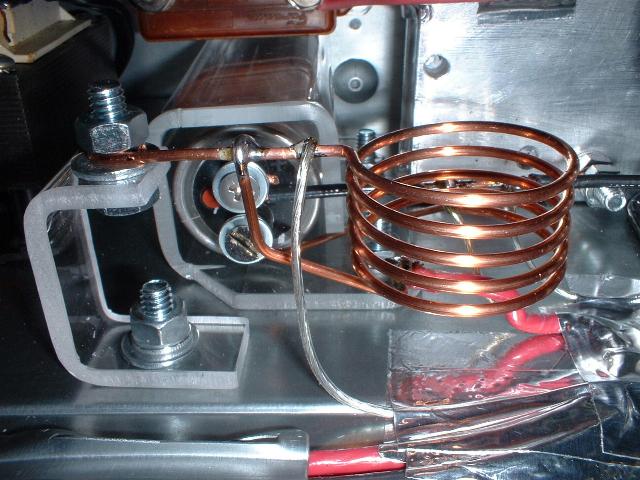
This is not an RF coil, it is a resistor!
More specifically, it is a meter shunt which makes the front panel meter read full scale when 30 amperes flows through it. It is used to read the PA Drain Current. It consists of two feet of #12 copper wire wound up in a convenient coil. It is insulated from the chassis by the plastic support shown to the left of the shunt coil.
Copper wire is not the best material to use for a shunt resistor, since it has a rather large positive temperature coefficient, but when operating over the limited room temperature range encountered here, the results are acceptable. The self-heating of the wire at the amplifier's normal current draw of 20-24 amperes is low enough to cause no problems. The resistor is in the cooling air flow as well, so it maintains a stable temperature.

The PA transistors mounted on the heat sink.
The large bolts extending through the heat sink are 1/4" bolts. They are used to clamp the source leads of the transistors to the heat sink and connect to the negative side of the power supply. The transistors themselves are screwed down to the heat sink. Rubberized thermal pads are used between the transistors and the heat sink.
The black #12 wire coming from the PA output transformer is soldered to the center drain lead of the transistors. The #12 red wire goes to one side of the PA tank tuning capacitors.
Notice the twisted pairs of wires connecting to the left gate lead of the transistors. The silver wire actually carries the drive signal, and the copper wire is grounded, forming a twisted pair transmission line for preventing noise pickup in the drive signal leads. Note that these twisted lines are fastened down with Aluminum tape.
The drain shunt resistors are placed directly across the the gate and source pins of the transistors. The clear plastic bracket mounted between the transistors is the support for the PA output transformer.

The RF output waveform across the dummy load when no PA tank tuning capacitors are installed.
If the transmitter is operated without PA tank resonating capacitor C12 installed, this is what the RF signal looks like when the transmitter is properly loaded. The ringing is caused by stray resonances in the tank circuitry, and can be minimized by careful parts placement.
If the transmitter is underloaded, the flat top and bottom of the signal will be tilted so that the leading edge is higher than the trailing edge. The ringing will also increase. Conversely, if the transmitter is overloaded, the flat top and bottom of the signal will be tilted so that the leading edge is lower than the trailing edge. For a 50 ohm load, the normal tap position will be at 20 to 25 turns. For a 75 ohm load, the tap will position be between 25-30 turns.
Notice the angled drop-off of the trailing edges of the signal. This represents areas where the transistors are partially on, and therefore dissipating power as heat. This represents a substantial power loss, in the neighborhood of 150 to 150 watts. Resonating the PA tank transformer reduces the loss considerably and makes the waveform much closer to a sine wave.

A first try at tuning the PA transformer.
In this picture, we see that the PA transformer resonating capacitors have been connected. However, the capacitor value is a bit too small, and some of the "squareness" of the waveform still shows near the zero crossing points. There is also a considerable amount of stray ringing visible on the signal.

That's much better!
The tuning capacitor value has been increased enough so that all the remaining "squareness" has disappeared from the signal. The stray ringing has also diminished considerably, and the waveform approaches a sine wave.
It should be noted that both the loading tap switch setting and the value of the tuning capacitor C12 will affect the quality of the waveform. In general, just as with a conventional vacuum tube amplifier, you adjust the tuning capacitor for minimum drain current, and adjust the loading switch for maximum output. For best results, watch the signal on an oscilloscope and tune and load for the best waveform and highest efficiency. The exact value of C12 is not extremely critical.
Note that this waveform is still not clean enough to be placed on the air. In order to meet FCC regulations, a low-pass filter must be used between the transmitter and the antenna.

Here's the finished transmitter in service.
( Ignore the mess! )
The power supply is on top of the transmitter, and below the transmitter is the computer which runs NT4.0 and ARGO for receiving, and WinAmp for generating the audio control signals for the transmitter ID loops. Since this picture was taken, a CD player has replaced the computer for running the ID loop. The low pass filter is on the floor (not visible), directly beneath the control computer.

A closer view of the transmitter in operation.
PA drain current is about 20 amperes at 24 volts. Power output is 400 watts from the low pass filter network. Since this picture was take, an air filter has been added to the fan, and another coax jack has been added between the meter and the meter switch for external FSK control.
As of 7 NOV 2002, the transmitter has accumulated over 2,500 on-the-air hours at full power with no failures. ( I exclude the operator-induced failure of one PA transistor caused by placing a dead short across the primary of the PA transformer while running at full power. )
73, Ralph W5JGV
[Home]
The entire contents of this web site are Copyright © 2002 by Ralph M. Hartwell II, all rights reserved.