Experimental KW Switching Power Supply
Initial Design and Test Report - Dec 28, 2003
By W5JGV
This is an ongoing narrative of my attempt to construct a high-power switching power supply to replace the failed power supply in my Heath Warrior amplifier. Since I use the amplifier for experimental (non-Ham) work, it sometimes has to operate at full CW power for several hours at a time. The original plate transformer is unsuitable for that task, so I am attempting to build a really heavy-duty supply to replace the original power supply.
My design concept started when I inherited a large quantity of well-built Dell computer power supplies. They were rated for 230 watts, and some testing showed that the switching transformers in the supplies could easily handle 250 watts. Hmm... If there was just a way that I could make these things put out HV instead of +5 Volts, I'd be all set. Well, to work!
I started by reverse engineering the supplies, and soon had a rough schematic diagram sketched out. It was quite simple, really. When the supply operates on 120 Volts, half of a full wave bridge rectifier charges a pair of filter capacitors to + and - 150 Volts, respectively. These voltages are alternately switched across the primary winding of the power supply transformer by a pair of transistors connected in a "totem pole" configuration (A half-bridge" circuit.) The secondary windings produce various voltages which are rectified, filtered and distributed to the loads in the computer. Samples of the +5 and +12 volt output are used for feedback to the voltage regulator circuitry.
Unlike the series pass regulators most of us are familiar with, computer power supplies use a pulse-width modulation system to vary the output voltage. Another difference between computer power supplies and the "big iron" hams use if that these supplies use a switching frequency of something in the neighborhood of 25 KHz. This allows the use of a much smaller power transformer than if the operating frequency were 60 Hz. This means that a lot of watts can be pushed through a very small transformer. These particular power supplies use a Texas Instruments TL494 Pulse Width Modulator (PWM) IC (16 pin DIP). Identical substitutes are the Fairchild KA7500B and the NTE 1729.
Because of the high switching frequencies as compared to 60 Hz, it is necessary to use fast diodes for rectification. I used UF4007 diodes, obtained on eBay. These are the same as the venerable 1N4007 but a heck of a lot faster in recovery time.
Then power supplies were decomposed into a pile of useful parts. Some of the diodes were used, as were the main 150 Volt filter capacitors. Interestingly enough, the original power switching transistors, which originally handles 230 watts, were rated high enough to easily handle a full KW. Tests showed that they could, in fact, handle that power level. (Barring the authors' ham-handedness with clip leads - see the picture further down the page.) One fan was pressed into service to cool both the main power rectifier and the switching transistor heat sink. All of the 150 Volt filter caps from six of the computer power supplies were ganged together to make up the main filter cap bank. A time delay start circuit was added to handle inrush current surges. ( A primary line noise & RF filter network will be used on the finished product.)
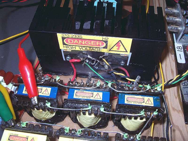
The switching transformer(s) deserve some mention here. The step up transformer is a actually a set of six computer power supply transformers, all having their primary windings connected in series. This becomes the high voltage secondary winding; it's just distributed across six transformers instead of one. The primary winding, which is connected to the switching power transistors, consists of the windings which were originally used to supply the +5 volts from the computer supplies. These windings are wound 5-0-5 volts for a full wave rectifier connection. I abandoned the center tap of the windings, and connect power across the entire winding. All six of the transformers have their 5-0-5 windings connected in series. The high voltage secondary winding is composed of the original primary windings, all of which are also connected in series. Although this works, there appear to be some voltage breakdown problems (All the Magis Smoke) escaped from one of the series-connected transformers during an overpower test) and it may be necessary to go to a single transformer instead of series-connected units. More on this later, as I figure it out.
OK, let's start with some pictures...
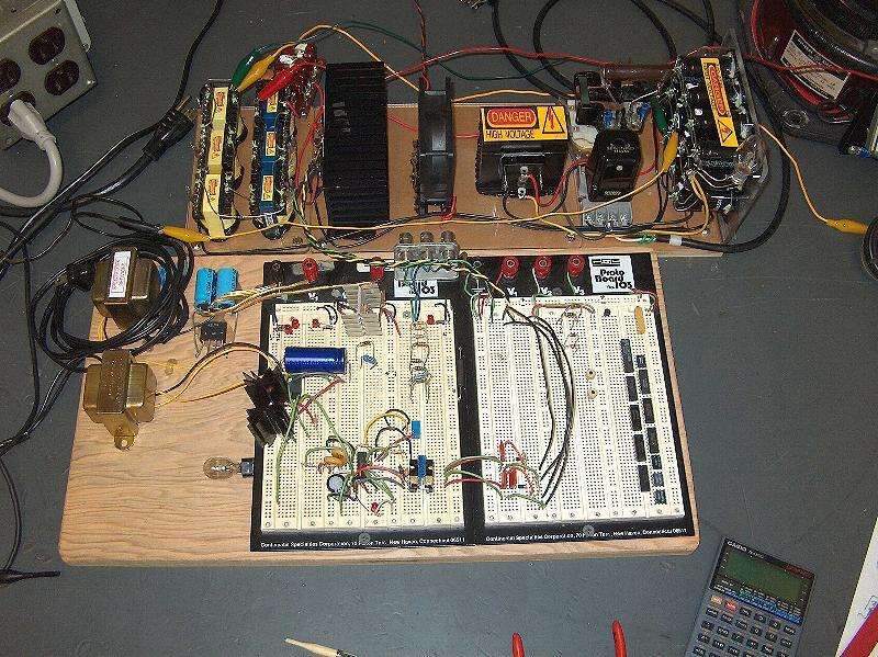
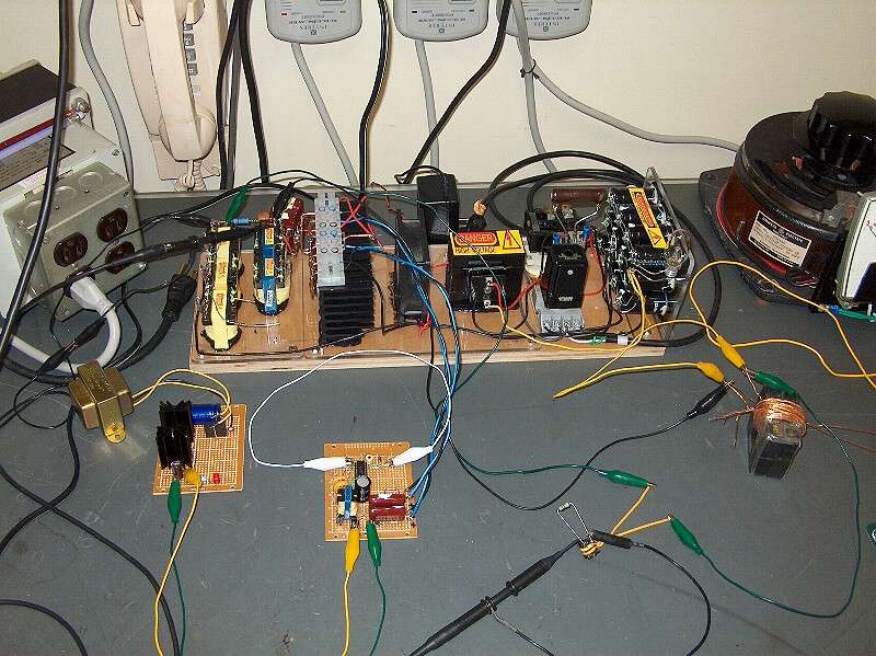
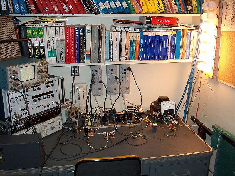
This is an overall view of the test setup. At the far upper right of the picture, you can see the 16 ampere Variac I use to help keep the smoke inside the components. At the far upper left of the picture you can see the outlet box on my 2.5 KVA isolation transformer, which helps keep the smoke inside of me and my test equipment. In the top center of the picture is the guts of the switcher system.
Starting from the left of the unit, you can see the set of six transformers which have been taken from the computer power supplies. The green paint on the connections indicates that I have visually and mechanically inspected the solder connections before applying power. To the right of the transformers is a black heat sink, salvaged from a Pentium-II processor. The power switching transistors are located on the back of the heat sink where the wires connect to the transistors. To the right of the P-II heat sink is a fan, also taken from one of the computer power supplies. It is powered by a 9 volt, 450 MA wall-wart purchased at the thrift store for 50 cents. After some experimentation, I found that a spacing of 1 inch from the heat sink gave the best cooling and the most even heat distribution across the heat sink. Closer or further spacing results in uneven cooling. The fan also sucks some air past the heat sink just to the right of the fan - the one with the "DANGER- HIGH VOLTAGE" label on it. That heat sink came from a cast-off Pentium PRO processor, and now does duty as the cooling device for the 30 amp bridge rectifier you can see bolted to the front of the heat sink. Regarding the bridge rectifier - I only use two legs of the bridge, and the current is low enough that I could have used one of the bridge rectifiers from one of the power supplies instead, but I had this one available.
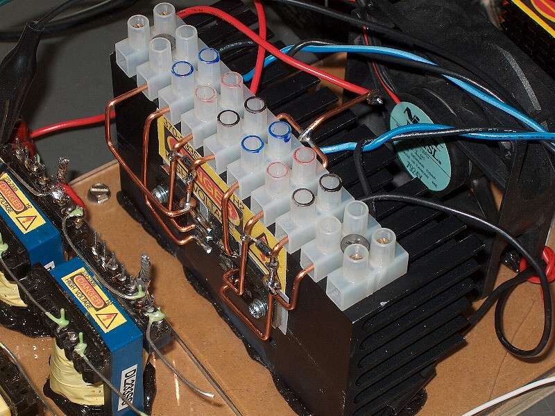
To the right of the diode bridge is a black time delay relay mounted on a gray octal socket. This relay closes the NO contacts two seconds after application of primary AC power, and causes the 30 amp power relay (partially seen behind the TD relay) to close its NO contacts, shorting out the 20 Ohm 50 watt Ohmite power resistor seen standing up horizontally above the power relay. The Ohmite resistor is in series with the AC liner and acts as surge protection to allow the 300 volt filter cap bank charge up without popping the line fuses.
At the far right of the setup is the filter cap bank, consisting of 12 - 680 MFD 200 VDC electrolytic, salvaged from the computer power supplies. They are arranged as two sets of 6 caps, wired in series, to provide an equivalent value of 2040 MFD @ 400 VDC. (2 X 4080 MFD @ 200 VDC) A "visual bleeder" is provided in the form of a 4-watt light bulb connected across each half of the capacitor banks. The final version will have two bulbs in series across each side of the capacitor bank to reduce the chance of lamp failure. There's some serious energy stored in that setup - it takes close to 30 seconds for the lamps to go out after the power is shut off!
Looking at the white double breadboard in the lower part of the picture, if you draw a line horizontally across the breadboard just above the large blue electrolytic cap on the left breadboard, nothing above the cap is connected to the system. The small power transformer to the left - the one without a label - supplies power to a bridge rectifier and charged the big blue filter cap to ~30 VDC. This is regulated down to +17 VDC by an LM317 regulator which is mounted on the black finned heat sink seen at the far left of the white breadboard. The heat sink, of course, came from a computer power supply.
The assortment of parts seen at the lower middle of the left white breadboard composes the switching control circuit. The black IC - partly hidden by the thicket of wires - is a TL494 switching power supply controller. It came from - guess where - one of the computer power supplies. It's readily available from several suppliers, and costs under a buck. It consists of a sawtooth waveform generator followed by a J-K flip-flop driving a pair of output transistors that can handle 40 V @ 200 MA. A pair of DC level comparators connects to the innards of the ramp generator to vary the duty cycle of the output signal - which is a square wave, BTW - thus allowing the main switching transistors to conduct for however long is needed to provide the power required by the load. Of course, the designer has to provide the necessary feedback circuit to make this all work. (That's about 90% designed, and 0% tested!)
The few parts on the lower left of the right hand white breadboard are part of the base drive circuitry between the power transistors and the driver transformer, which is seen at the bottom right of the left hand white breadboard. Can you guess where the driver transformer came from? Right!!!
The voltage control feedback circuit will sample the +1500 volts at the output and send it to the TL494 comparator inputs. Over current sense will also be provided to shut down the supply in case of a HV load short or serious overload, such as an internal arc in a PA tube. At the bottom right of the picture is my best tool - my calculator. If the math says it will work, it will!
The smoke has seriously escaped from these power transistors! I was running the primary DC voltage at about 400 volts instead of 300 (to see what would happen - now I know!!) and I think I bumped the breadboard and accidentally hit something that caused both transistors to switch on at the same time. This picture also gives you a close up view of the jumper connections for the transformers. Like the warning labels? I scanned one (from a computer supply, of course) and printed a few of them out and stuck 'em on the various parts.
Ahh! That's much better! After replacing the switching transistors, I installed a nice heavy-duty terminal strip to make connections easy and positive for testing. The heavy copper wires help keep the transistor leads cool and are easy to unsolder and bend away slightly if it becomes necessary to replace the transistors (again!) Note the cut-off bare wire from the transformer in the lower left of the picture. it went to the transformer that smoked while testing at high power. The transformer has been removed and dissected to determine the cause of failure.
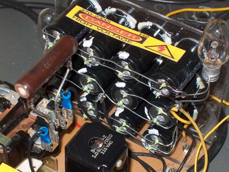
A close-up view of the main filter capacitor bank. It consists of 12 caps, each rated at 680 MFD @ 200 VDC. They are arranged as a two sets of six of these caps in parallel, with both sets in series. The series set is then charged to +/- 150 VDC through half of a 30 Ampere 600 Volt bridge rectifier directly from the power line. The brown Ohmite power resistor is the inrush current limit resistor. The small "night light" lamp is a self-indicating bleeder resistor. There is one across each set of filter capacitors. The final version of the supply will have two of these lamps in series across each set of capacitors for higher reliability.
The breadboard setup after the +17 Volt power supply and the Switcher Driver circuits had been finalized and assembled on perf boards. note the missing transformer from the main prototype setup. At this point, all six of the switcher transformers are out of the circuit and have been replaced by the single hand-wound prototype transformer visible at the far right of the picture. The scope probe is connected to a current sample transformer that generates a signal proportional to the current from the main switching transistors to the transformer. This will eventually be used to perform an instant shutdown of the system in the event of a serious overload.
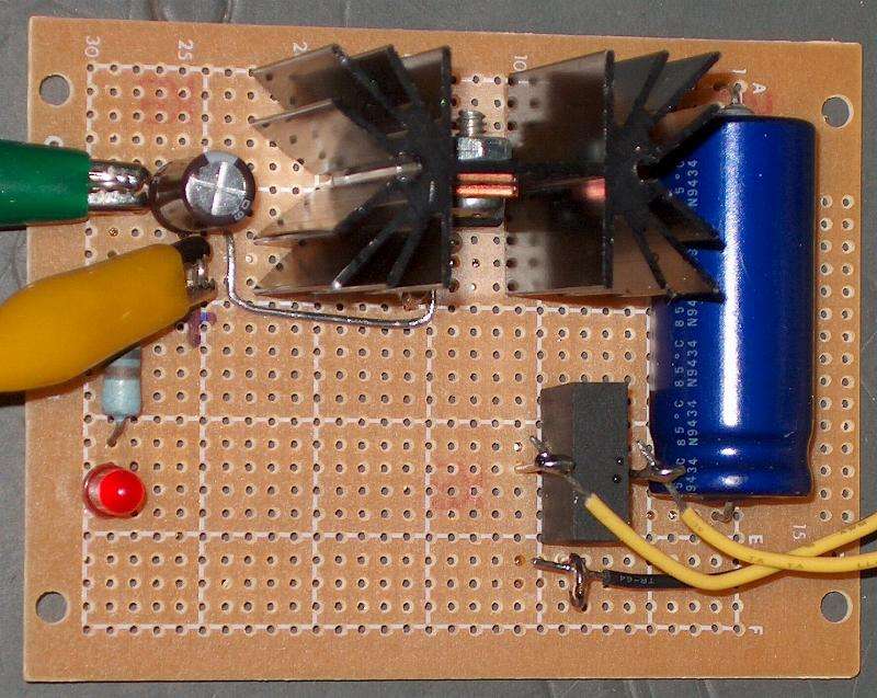
The completed +17 volt power supply. A 24 VAC @ 450 MA transformer (yellow leads) drives a bridge rectifier (black rectangle) and charged the big blue filter cap to about +30 VDC. An LM317T regulator mounted on the finned heat sink, produces +17 Volts @ 300 MA for the switcher control board. An LED provided a visual indication that the supply is working. I used a fixed resistance voltage divider to set the output of the regulator, so, no adjustment is supplied. It either works right or it's dead!
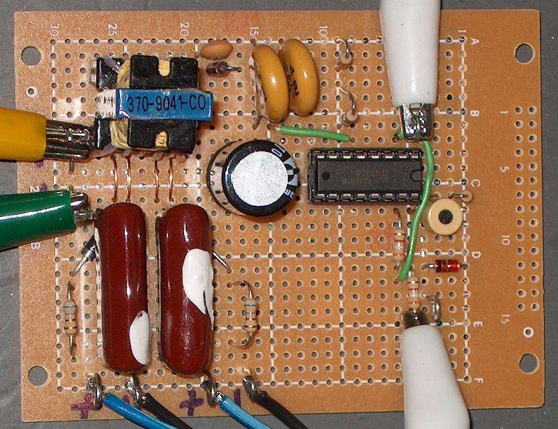
This is the completed switcher control board. The IC is the TL454. The large yellow disk caps and the two resistors adjacent to them provide frequency control, in this case, 50 KHz. (The IC divides by two, so the actual square wave output is at 25 KHz.) The output stage of the IC drives the small transformer (370-9041-CO) and was used in one of the computer power supplies to drive the main switcher transformers. I decided not to reinvent the wheel, so to speak, and swiped the circuit for use here. The two large brown capacitors are 2 MFD each, and along with the diodes (partially hidden under the caps) and the two resistors, form the base drive matching circuits needed to connect the transformer secondary windings to the bases of the main switching transistors. The black and blue wires connect to the switching transistors. The green and yellow clip leads provide the +17 Volts to the board. The two white clip leads are for regulation feedback, and are not functional in the present setup. The small beige potentiometer and the adjacent components are the voltage feedback adjustment network.
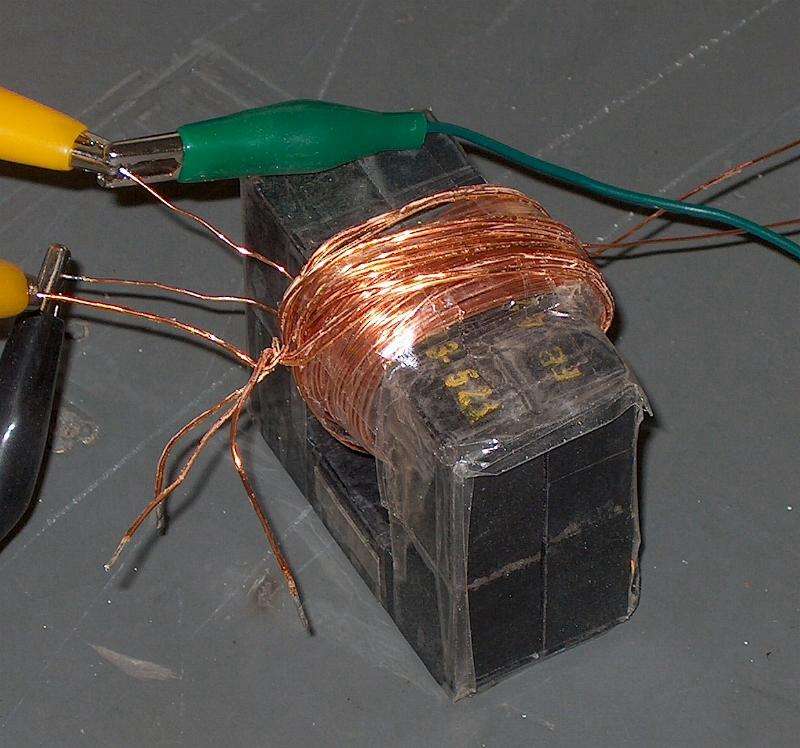
A quick-and-dirty lash-up of a homebrew switching transformer. I used a pair of ferrite cores from a couple of large LOPT (horizontal output transformers) stacked side by side and scramble wound what I calculated was the right number of turns on the core. Insulation is a few wraps of Cellophane tape! Certainly not recommended for long-term use, but good enough for a quick test. Each core measures about 0.5 x 0.4 inches thick. The exact core material is unknown, but since these transformers originally operated in the same frequency range as I am using, I thought they would probably work well enough for testing. They did.
The last picture! The prototype supply driving the incandescent lamp load. There are a total of 10 - 100 watt lamps brightly illuminated - you do the math. Note that all that power is coming through the home-brew junk-box transformer I wound. The switching waveforms are visible on the oscilloscope, if a bit hard to make out. The lower waveform is the switching transformer primary current, and the upper waveform is the load voltage. It's AC, since the HV rectifiers have not been installed yet. Switching frequency is 25 KHZ, and the duty cycle is about 98%.
I'll post more info as I get things figured out.
73,
Ralph W5JGV